Semiconductor chip package having decoupling capacitor and manufacturing method thereof

a semiconductor and capacitor technology, applied in the field of semiconductor chip packaging, can solve the problems of noise and signal propagation delay, performance degradation, diminishing the beneficial effect of decoupling capacitors, etc., and achieve the effects of improving the decoupling capacitor, reducing parasitic resistance and inductance, and shortening the path to a semiconductor devi

Active Publication Date: 2006-10-31
SAMSUNG ELECTRONICS CO LTD
View PDF14 Cites 42 Cited by
  • Summary
  • Abstract
  • Description
  • Claims
  • Application Information

AI Technical Summary

Benefits of technology

[0007]Exemplary, non-limiting embodiments of the present invention may provide a semiconductor chip package having an improved decoupling capacitor, which has a shorter path to a semiconductor device, reduced parasitic resistance and inductance, and easy capacitance adjustability.

Problems solved by technology

Along with the fast clock speed of semiconductor devices, noises and signal propagation delay are becoming important issues that must be addressed.
Power / ground noises may be caused by parasitic inductance in high-speed semiconductor devices and / or a package substrate.
The power / ground noise leads to increasing signal delay that may result in performance degradation.
This may diminish the beneficial effects of the decoupling capacitors.
This may raise difficulty in choosing the decoupling capacitors.

Method used


Image

  • Semiconductor chip package having decoupling capacitor and manufacturing method thereof
  • Semiconductor chip package having decoupling capacitor and manufacturing method thereof
  • Semiconductor chip package having decoupling capacitor and manufacturing method thereof

Examples


first exemplary embodiment

[0022

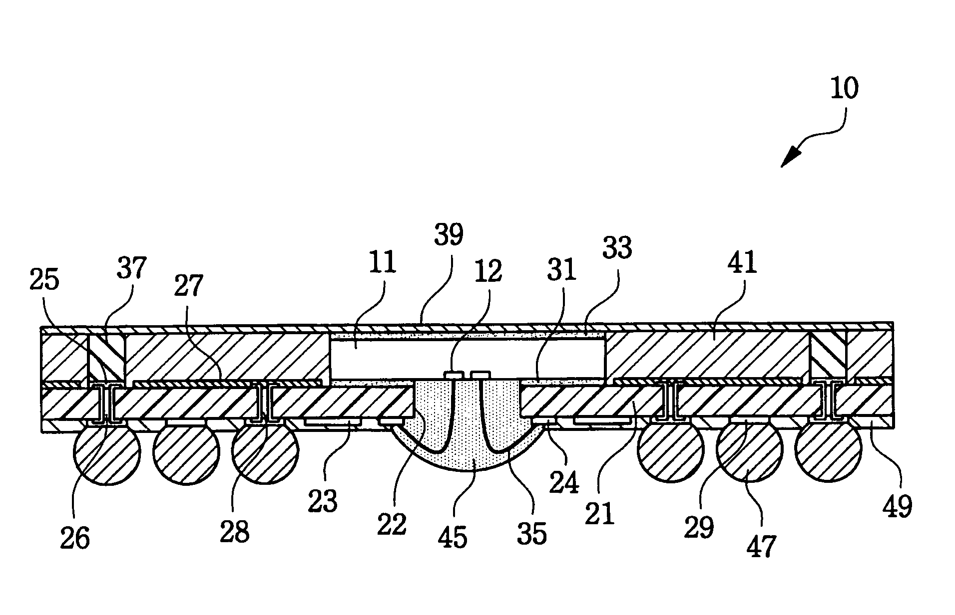
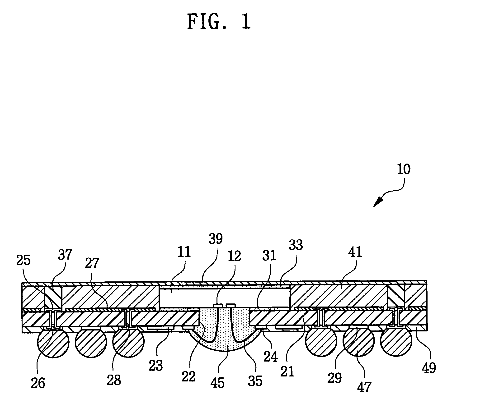
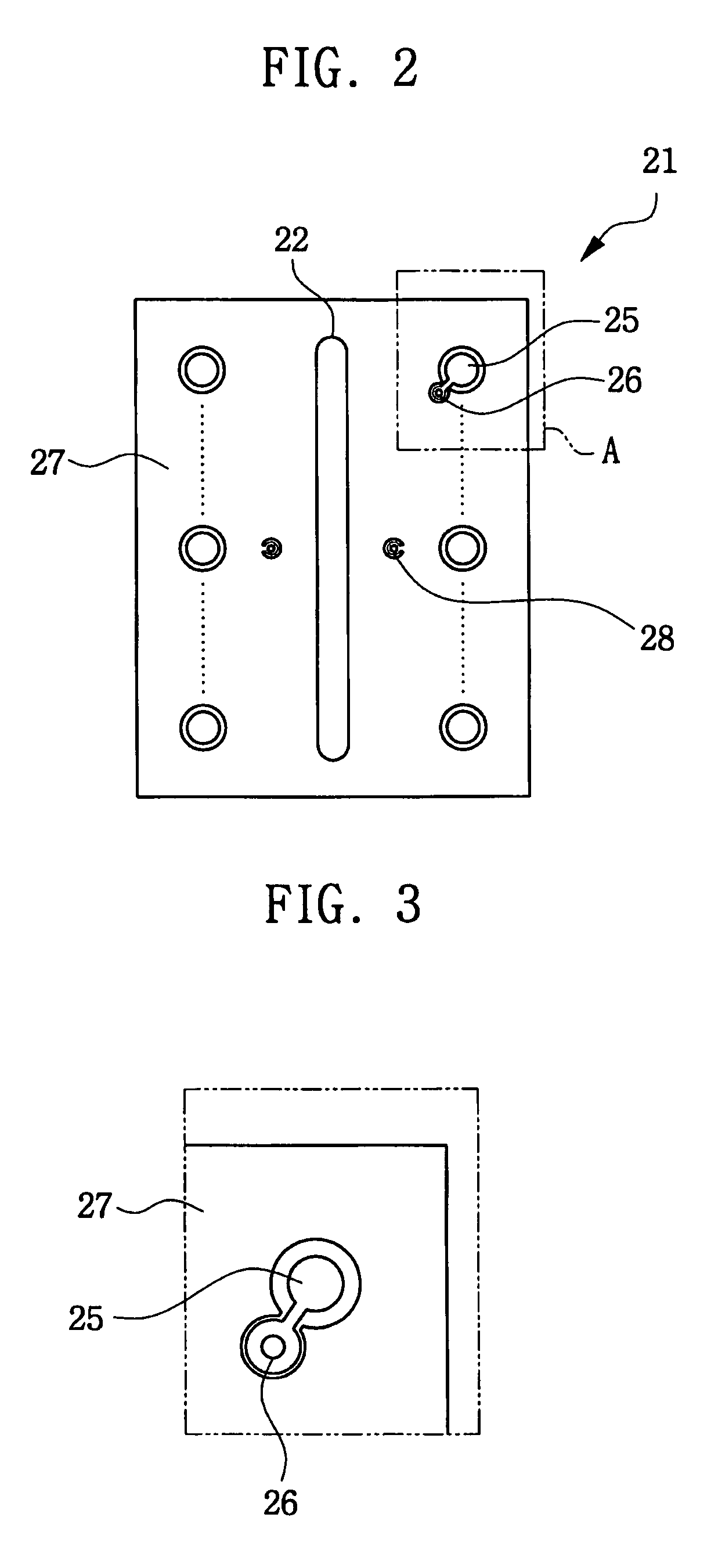
[0023]FIG. 1 illustrates, in a cross-sectional view, a semiconductor chip package 10 in accordance with a first exemplary embodiment of the present invention. Further, FIG. 2 illustrates a plan view of a substrate 21 as used in the semiconductor chip package 10 shown in FIG. 1; and FIG. 3 shows an enlarged view of section “A” in FIG. 2.

[0024]Package 10 includes a semiconductor chip 11 of a center pad type. That is, chip pads 12 are formed along a central line on an active surface of chip 11. The active surface of the chip 11 faces a substrate 21 and is attached thereto. The chip pads 12 of chip 11 are electrically coupled to the substrate 21 through bonding wires 35. Solder balls 47 are formed on the substrate 21 and are used as external connection terminals of the package 10. In particular, the package 10 has a decoupling capacitor composed of a power plane 27, a ground plane 39, and a dielectric layer 41.

[0025]The substrate 21 in this embodiment has an opening 22 formed in a ...

second exemplary embodiment

[0041

[0042]FIG. 5 shows, in a cross-sectional view, a semiconductor chip package 110 in accordance with a second exemplary embodiment of the present invention.

[0043]Referring to FIG. 5, a package 110 of this embodiment includes a semiconductor chip 111, which is attached to a substrate 121 in a flip-chip fashion through chip bumps 113. Solder balls 147 are formed under the substrate 121 and are used as external connection terminals of the package 110. The package 110 has a decoupling capacitor composed of a power plane 127, a ground plane 139, and a dielectric layer 141.

[0044]Instead of wire-bonding technique in the aforementioned embodiment, a flip-chip technique may be used to electrically connect the chip 11 and the substrate 121. Namely, the chip 111 and the substrate 121 are electrically connected through chip bumps 113 provided on chip pads (not shown). Chip bumps 113 are directly joined to substrate pads 124 disposed on the top surface of the substrate 121. Unlike the previou...

third exemplary embodiment

[0051

[0052]FIG. 7 shows, in a cross-sectional view, a semiconductor chip package 311 in accordance with a third exemplary embodiment of the present invention. Further, FIG. 8 shows, in a cross-sectional view, a substrate 421 exemplarily used in the package of this embodiment of the present invention, and FIGS. 9A and 9B show respectively, in plan views, top and bottom surfaces of the substrate 421 shown in FIG. 8.

[0053]Referring to FIG. 7, the package 311 of this embodiment includes two stacked semiconductor chips 311 and 411, which have chip bumps 312 and 412 and are attached to first and second substrates 321 and 421, respectively, in a flip-chip fashion through the chip bumps 312 and 412. Solder balls 347 are formed under the first substrate 321 and are used as external connection terminals of the package 310. The package 310 has two decoupling capacitors each composed of a power plane 327 and 427, a ground plane 339 and 439, and a dielectric layer 341 and 441.

[0054]The first chi...


PUM


Abstract

A semiconductor chip package has a substrate that includes circuit lines provided on first and / or second surfaces, a power plane provided on the second surface, bump lands provided on the second surface and coupled to the circuit lines, and ball lands provided on the first surface. The package further has a semiconductor chip attached to the second surface of the substrate and electrically coupled to the circuit lines, and a dielectric layer provided on the second surface of the substrate. The dielectric layer surrounds laterally the chip, covers the power plane, and exposes the bump lands. The package further has a ground plane provided on both the chip and the dielectric layer, vertical connection bumps provided within the dielectric layer and on the bump lands and electrically coupled to the ground plane, and solder balls provided on the ball lands.

Description

CROSS REFERENCE TO RELATED APPLICATIONS[0001]This application claims priority under 35 U.S.C. §119 to Korean Patent Application No. 2003-81531, filed Nov. 18, 2003, the contents of which are incorporated herein in its entirety by reference.BACKGROUND OF THE INVENTION[0002]1. Field of the Invention[0003]The present invention relates generally to electronic packaging technology and, more particularly, to a semiconductor chip package having an improved decoupling capacitor and a method for manufacturing the semiconductor chip package.[0004]2. Description of the Related Art[0005]Along with the fast clock speed of semiconductor devices, noises and signal propagation delay are becoming important issues that must be addressed. Power / ground noises may be caused by parasitic inductance in high-speed semiconductor devices and / or a package substrate. The power / ground noise leads to increasing signal delay that may result in performance degradation.[0006]The employment of decoupling capacitors ...

Claims


Application Information

Patent Timeline
Patent Type & Authority Patents(United States)
IPC IPC(8): H01L23/02H01L23/13H01L23/12H01L23/24H01L23/48H01L23/498H01L23/50H01L23/538H01L25/065H01L25/07H01L25/18
CPCH01L23/13H01L23/49838H01L23/50H01L23/5383H01L25/0657H01L2224/06136H01L2224/48091H01L2224/4824H01L2224/73215H01L2225/06517H01L2225/06541H01L2225/06551H01L2225/06572H01L2225/06582H01L2924/01057H01L2924/15153H01L2924/1517H01L2924/15311H01L2924/19041H01L2924/30107H01L23/24H01L2224/0401H01L2224/73253H01L2224/32245Y10S257/924H01L2224/32225H01L2224/16225H01L24/48H01L2924/00014H01L2924/00H01L2224/45099H01L2224/45015H01L2924/207H01L23/48
Inventor KANG, SUN-WON
Owner SAMSUNG ELECTRONICS CO LTD
Why Eureka
Try Eureka