Power supply packaging system

a power supply and packaging technology, applied in the field of power transistor packaging, can solve the problems of less room within the power supply package for dissipating the heat generated by the device, the power semiconductor device tends to generate substantial amounts of heat, and the power supply package is not large enough to meet the needs of power supply applications, and achieves improved heat exhaust path, large full package dimension, and thin module package

Inactive Publication Date: 2006-10-31
BEL POWER SOLUTIONS INC
View PDF17 Cites 13 Cited by
  • Summary
  • Abstract
  • Description
  • Claims
  • Application Information

AI Technical Summary

Benefits of technology

[0007]The present invention is a novel package design for high current power supplies, which improves upon the prior art by providing for an improved heat exhaust path for the high current FET switches, while having a very thin module package. The heat exhaust path is from the drain electrode formed on the back side

Problems solved by technology

Future processors may consume current at levels an order of magnitude higher than today's processors, and will dissipate much more power because the operating voltage will not decrease proportionately.
Power semiconductor devices tend to generate substantial amounts of heat, because they are required to switch large currents.
However with the miniaturization of electronics products, less room exists within the power supply packages for dissipating the heat generated by the devices.
The requirements for packagin

Method used


Image

  • Power supply packaging system
  • Power supply packaging system
  • Power supply packaging system

Examples


Embodiment Construction

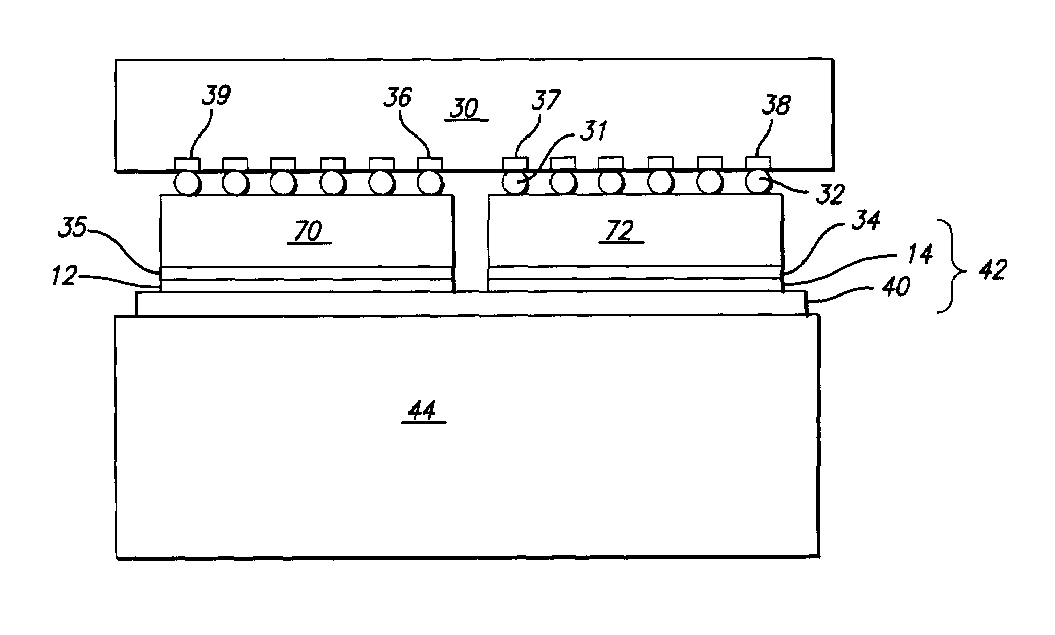
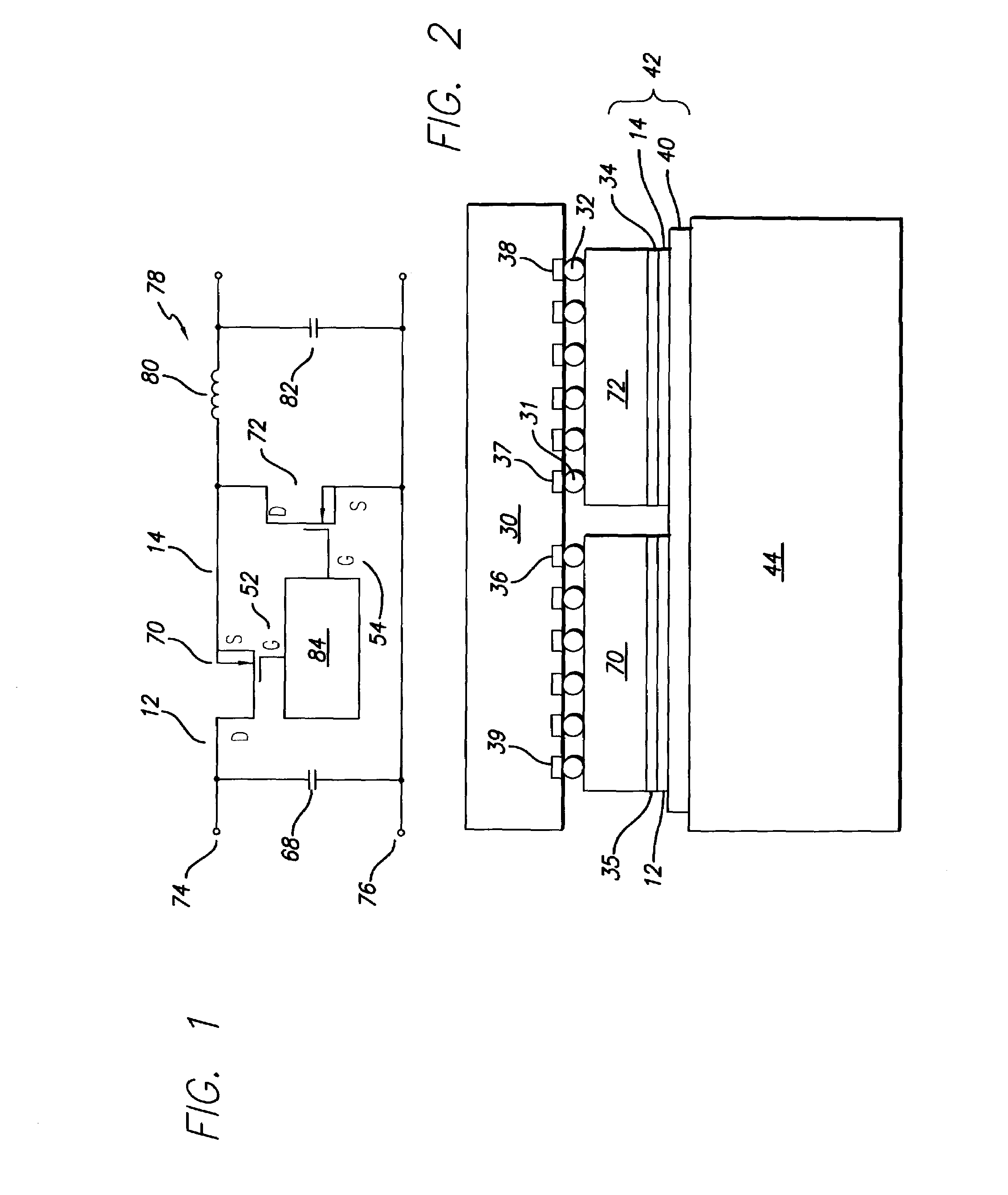
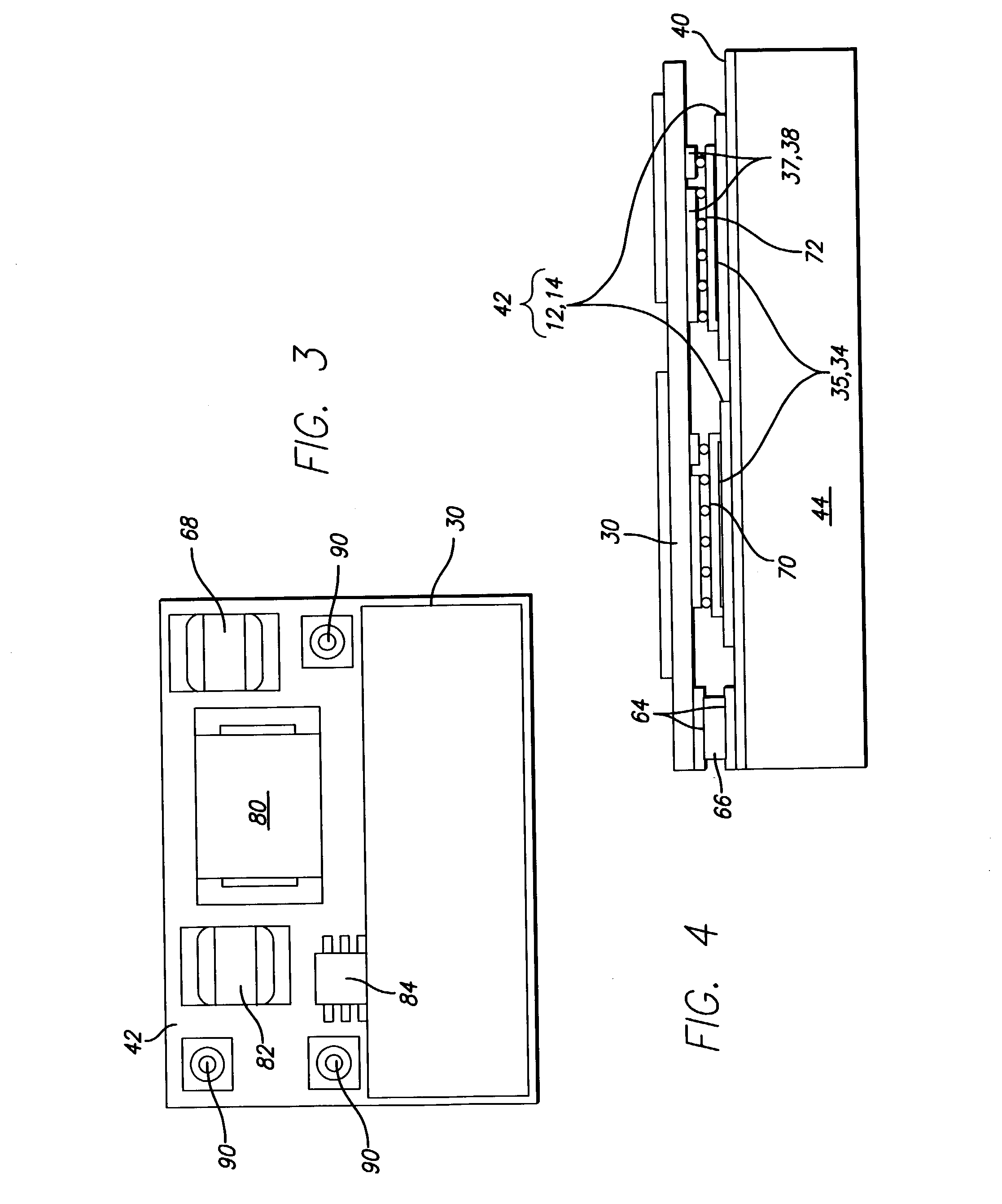
[0020]Chip-scale packages (CSPs) have become common in the electronics field, as a result of efforts to minimize the physical size of the component. Chip Scale Packaging is generally defined as a single die package that is no larger than 1.2 times the die size. A CSP is often designed such that the integrated circuit die is attached to its mating surface, generally a printed circuit board, face-down, with the chip pads connecting to the PCB pads through individual balls of solder. The CSP approach to semiconductor packaging takes up a minimal amount of additional volume, by using direct solder ball attachment and leaving some or all surfaces of the bare chip exposed. The principle advantages of the CSP are a reduction in package size and enhanced thermal conduction characteristics, as well as a reduction in the chip-to-PCB inductance.

[0021]Alternatively, an FET die with a solderable source electrode can be used with a metallic strap (relatively wide, thick member for low resistance)...


PUM


Abstract

A packaging system for a high current, low voltage power supply. The power supply uses bare die power FETs which are directly mounted to a thermally conductive substrate by a solder attachment made to the drain electrode metallization on the back side of the FETs. The source electrode and gate electrode of each FET are coupled to the circuitry on an overhanging printed circuit board, using CSP solder balls affixed to the front side of the FET die. The heat generated by the FETs is effectively dissipated by the close coupling of the FETs to the thermally conductive underlying substrate.

Description

FIELD OF THE INVENTION[0001]The present invention relates to the packaging of semiconductor devices. More particularly, this invention relates to the packaging of power transistors to form a power supply.BACKGROUND OF THE INVENTION[0002]With the advent of microprocessors and other electronics that consume more electrical power, comes the need for higher output power supplies. While microprocessor voltage requirements are decreasing, substantial increases in electric current requirements are offsetting this trend. Future processors may consume current at levels an order of magnitude higher than today's processors, and will dissipate much more power because the operating voltage will not decrease proportionately. GHz class central processing units (CPUs) are routinely specified to draw 30A or more of direct current. Therefore a need has arisen for high current, low voltage power sources which have a small physical size and generate a modest amount of heat. (As is conventional, “power ...

Claims


Application Information

Patent Timeline
IPC IPC(8): H01L23/10H01L23/34H01L23/538H01L25/11H05K1/02H05K1/14H05K1/16
CPCH01L23/5385H01L25/115H05K1/0203H05K1/165H01L2924/1305H05K1/145H05K2201/086H05K2201/09063H05K2201/1056H05K2201/10674H01L2224/16225H01L2924/19105H01L2224/32225H01L2224/73253H01L2924/00
Inventor MAXWELL, JOHN A.
Owner BEL POWER SOLUTIONS INC
Why Eureka
Try Eureka