Simultaneous multi-spot inspection and imaging

a multi-spot inspection and imaging technology, applied in the field of surface inspection, can solve the problem of increasing the amount of time required for the spot to scan over the entire surface, and achieve the effect of enhancing the sensitivity of detection and enhancing performan

Inactive Publication Date: 2006-10-31
KLA TENCOR TECH CORP
View PDF8 Cites 101 Cited by
  • Summary
  • Abstract
  • Description
  • Claims
  • Application Information

AI Technical Summary

Benefits of technology

[0013]In yet another embodiment, the same optics is used for focusing illumination beams of radiation to an array of spots on a surface and for imaging scattered radiation from the spots onto corresponding receivers or detectors in an array. The optics has an aperture where the illumination beams are focused through a first portion of the aperture and the ima

Problems solved by technology

This means that the amount of time required for the spot to s

Method used


Image

  • Simultaneous multi-spot inspection and imaging
  • Simultaneous multi-spot inspection and imaging
  • Simultaneous multi-spot inspection and imaging

Examples


Embodiment Construction

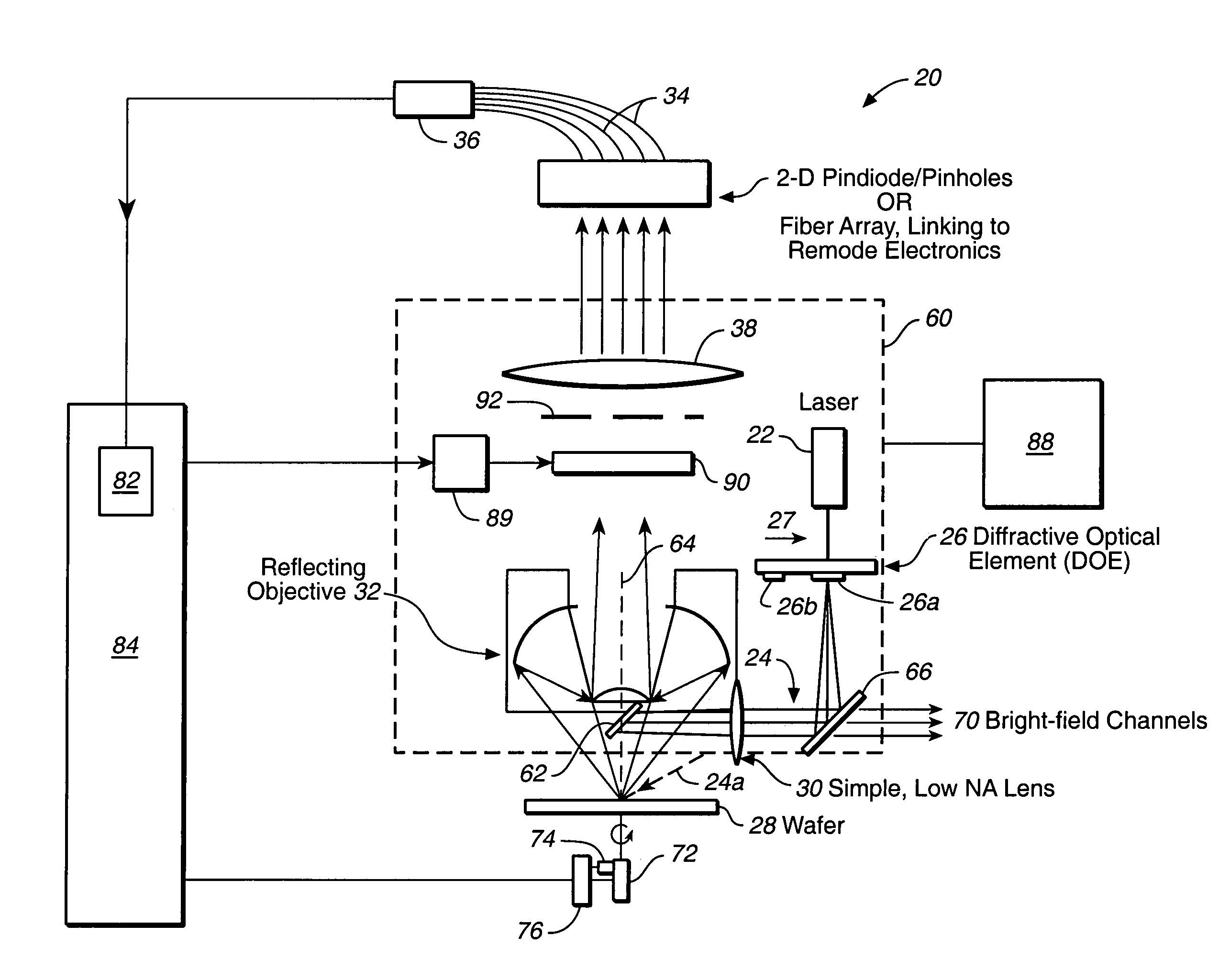
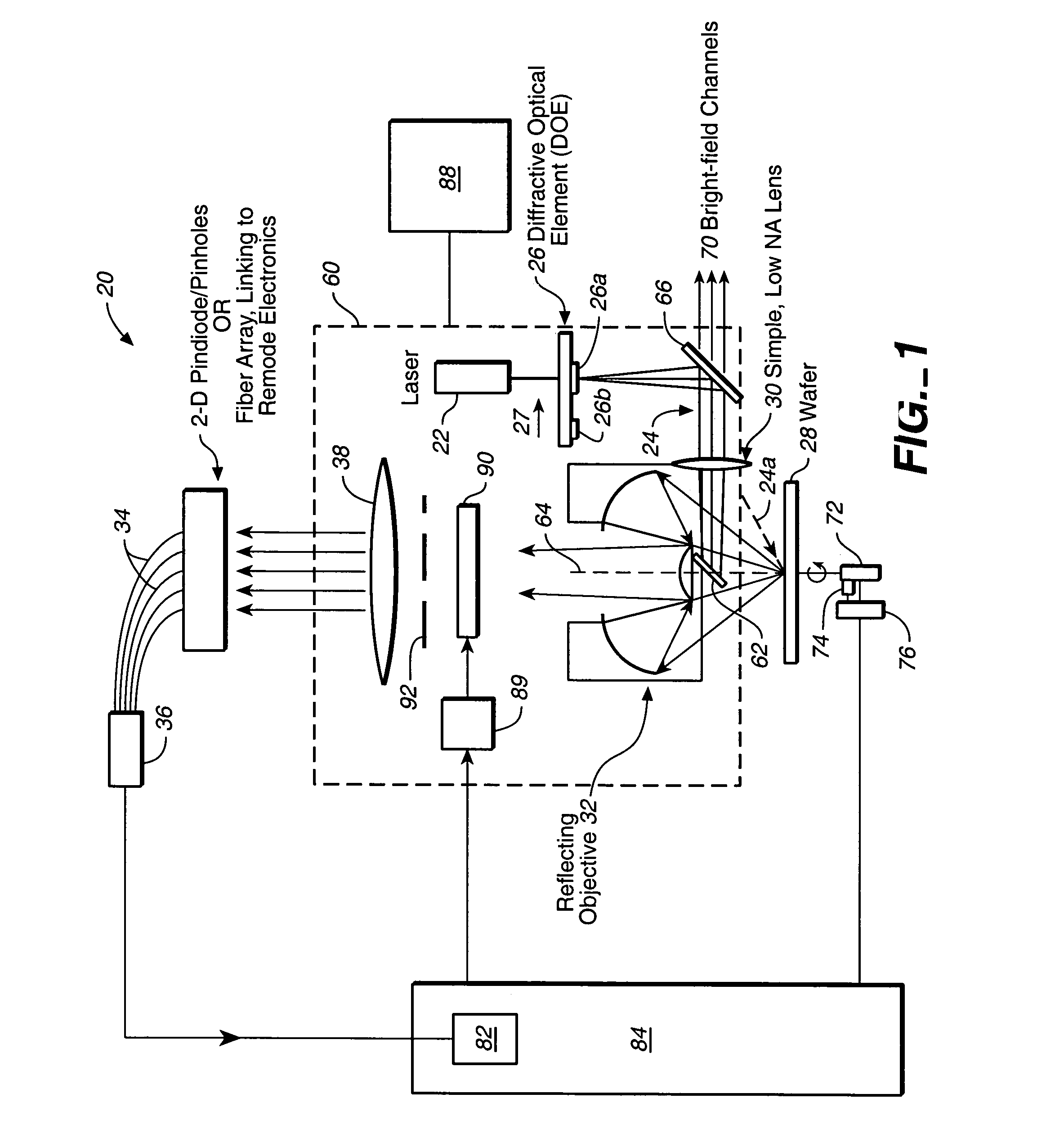
[0026]The costs associated with dark-field pattern inspection has increased steadily with enhanced performance. As semiconductor fabrication approaches finer design rule and resolution, the complexity of inspection tasks has increased dramatically, which, in turn, increases the complexity and costs of the optical front end of the inspection tool and of detection electronics. Furthermore, the variety of situations calling for optical inspection means that a versatile optical inspection tool is preferably compact, rugged and has a small foot print so that it is less sensitive to vibrations, and integratable with semiconductor processing equipment. Preferably, the system can be used for inspecting surfaces with diffracting patterns thereon such as patterned wafers, as well as surfaces without such patterns such as unpatterned semiconductor wafers. The embodiments of this invention also enable faster and more sensitive inspection to be performed at a reasonable cost.

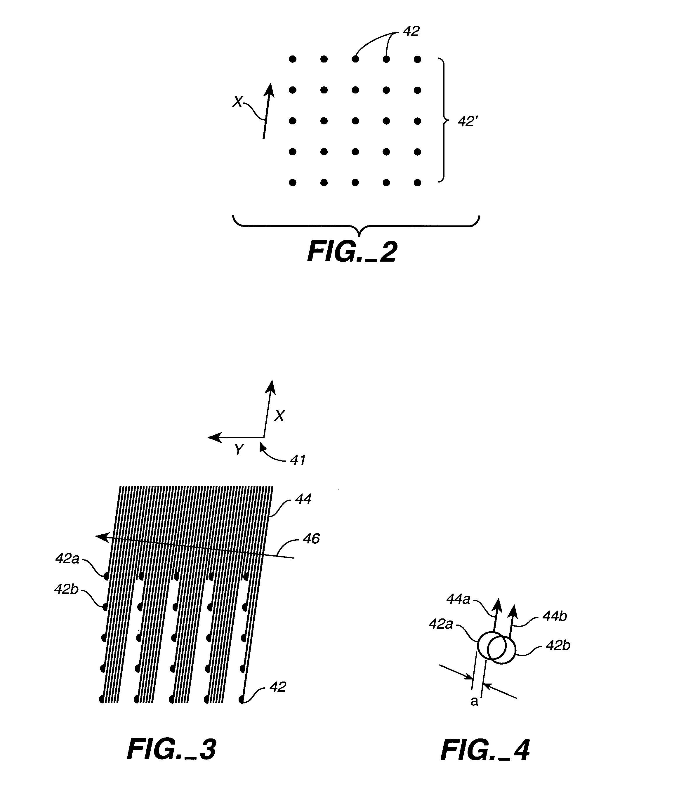
[0027]The elements o...


PUM


Abstract

A compact and versatile multi-spot inspection imaging system employs an objective for focusing an array of radiation beams to a surface and a second reflective or refractive objective having a large numerical aperture for collecting scattered radiation from the array of illuminated spots. The scattered radiation from each illuminated spot is focused to a corresponding optical fiber channel so that information about a scattering may be conveyed to a corresponding detector in a remote detector array for processing. For patterned surface inspection, a cross-shaped filter is rotated along with the surface to reduce the effects of diffraction by Manhattan geometry. A spatial filter in the shape of an annular aperture may also be employed to reduce scattering from patterns such as arrays on the surface. In another embodiment, different portions of the same objective may be used for focusing the illumination beams onto the surface and for collecting the scattered radiation from the illuminated spots simultaneously. In another embodiment, a one-dimensional array of illumination beams are directed at an oblique angle to the surface to illuminate a line of illuminated spots at an angle to the plane of incidence. Radiation scattered from the spots are collected along directions perpendicular to the line of spots or in a double dark field configuration.

Description

CROSS-REFERENCE TO RELATED APPLICATIONS[0001]This application is a continuation-in-part of U.S. patent application Ser. No. 10 / 125,906, filed Apr. 18, 2002 (now abandoned), and also claims benefit of U.S. Provisional Patent Application No. 60 / 426,577, filed Nov. 15, 2002.BACKGROUND OF THE INVENTION[0002]This invention relates in general to the inspection of surfaces to detect anomalies, and in particular, to an improved system that illuminates the surface inspected at the plurality of spots simultaneously for anomaly detection.[0003]Conventional optical inspection methods employing scanning techniques typically causes a single spot on the surface inspected to be illuminated where the spot is scanned over the entire surface for anomaly detection. For improved signal-to-noise ratio caused by background scattering, the size of the illuminated spot has been continually reduced. This means that the amount of time required for the spot to scan over the entire surface is increased which is...

Claims


Application Information

Patent Timeline
IPC IPC(8): G01N21/68G01N21/88G01N21/956
CPCG01N21/8806G01N21/95623
Inventor VAEZ-IRAVANI, MEHDIMILLER, LAWRENCE ROBERT
Owner KLA TENCOR TECH CORP
Why Eureka
Try Eureka