Method for fabricating single crystal silicon film

a technology of silicon film and single crystal, which is applied in the direction of crystal growth process, polycrystalline material growth, chemistry apparatus and processes, etc., can solve the problem of limiting the number of switching devices required in lcd, the inability to achieve high speed with a-si tft, and the uniformity of grain distribution

Active Publication Date: 2006-11-14
BOE HYDIS TECH
View PDF3 Cites 68 Cited by
  • Summary
  • Abstract
  • Description
  • Claims
  • Application Information

AI Technical Summary

Benefits of technology

[0031]Accordingly, an object of the present invention is to provide a method for fabricating a single crystal silicon film, by which the crystallinity of low temperature poly-sil...

Problems solved by technology

Since a-Si TFT using a-Si has a very low mobility of about 0.5 cm2/Vs, there is a limitation in making all switching devices required in LCD, using a-Si TFT.
This is because a switching device for a peripheral circuit of LCD needs to be operated at a very high speed, but this high speed cannot be achieved with a-Si TFT.
Thus, it is preferred to obtain ELA conditions where the greatest possible size of grains can be obtained, but the greater the size of grains, the worse the uniformity of grain distribution.
This causes a degradation in uniformity of device characteristics, and as a result, causes a problem in view of reliability.
In this case, however, poly...

Method used


Image

  • Method for fabricating single crystal silicon film
  • Method for fabricating single crystal silicon film
  • Method for fabricating single crystal silicon film

Examples


Embodiment Construction

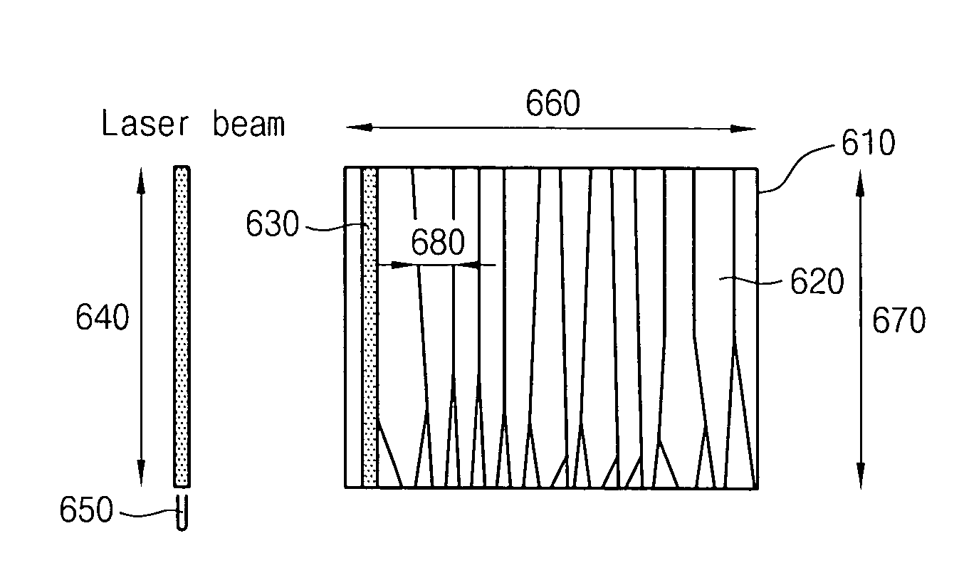
[0053]Hereinafter, a method for fabricating a single crystal silicon film according to the present invention will be described in detail with reference to the accompanying drawings.

[0054]In order to enhance crystallinity and also to ensure uniformity in forming a polycrystalline silicon (poly-Si) thin film on an amorphous substrate such as a glass or plastic insulator, a single crystal or a single-crystal tile whose location was precisely controlled is formed over the entire substrate according to the present invention. This allows problems of the prior art to be fundamentally solved. A typical method for this purpose is designed in the present invention, and the crystallization of a-Si will be described herein by way of example.

[0055]In a principle to realize the present invention, a poly-Si island pattern, which undergone the prior SLS process, is subjected to an additional laser scanning process in a perpendicular direction to a direction in which grains of the island pattern wer...


PUM


Abstract

The present invention relates to a method for fabricating a single crystal silicon thin film at the desired location to the desired size from an amorphous or polycrystalline thin film on a substrate using laser irradiation and laser beam movement along the substrate having the semiconductor thin films being irradiated. This method comprises the steps of: forming a semiconductor layer or a metal thin film on a transparent or semi-transparent substrate; forming a single crystal seed region on the substrate of the desired size by a crystallization method using laser irradiation; and converting the desired region of the semiconductor layer or metal thin film into a single crystal region, using the single crystal seed region.

Description

BACKGROUND OF THE INVENTION[0001]1. Field of the Invention[0002]The present invention relates to a method for fabricating a semiconductor thin film, and more particularly to a method for fabricating a single crystal silicon thin film at the desired location to the desired size from an amorphous or polycrystalline thin film on a substrate using laser irradiation and laser beam movement along the substrate having the semiconductor thin films being irradiated.[0003]2. Description of the Prior Art[0004]Generally, a thin film transistor (hereinafter, referred to as TFT), a core switching device, which is used in LCD or OLED using organic EL material, is the most important semiconductor device for the performance of a flat panel display (hereinafter, referred to as FPD).[0005]Mobility or leakage current, a measure of the TFT performance, greatly varies depending on the state or structure of a silicon (Si) thin film, which forms an active layer, a channel for charge carrier transport. In t...

Claims


Application Information

Patent Timeline
IPC IPC(8): H01L21/20H01L21/428C30B13/00H01L21/336H01L29/786
CPCC30B13/00H01L21/2026C30B29/06H01L21/02686H01L21/02678H01L21/02422H01L21/02381H01L21/02691H01L21/428
Inventor RYU, MYUNG KWANLEE, HO NYEONPARK, JAE CHULKIM, EOK SU
Owner BOE HYDIS TECH
Why Eureka
Try Eureka