Electrolytic copper plating method, phosphorous copper anode for electrolytic plating method, and semiconductor wafer having low particle adhesion plated with said method and anode
Active Publication Date: 2006-11-21
JX NIPPON MINING& METALS CORP
10 Cites 12 Cited by
AI-Extracted Technical Summary
Problems solved by technology
Nevertheless, when employing this electrolytic copper plate for forming copper wiring of semiconductors, a new problem arose which was not found in a PWB.
This is because when an insoluble anode formed from the likes of platinum, titanium, or iridium oxide is used, the additive within the plating liquid would decompose upon being affected by anodic oxidization, and inferior plating will occur thereby.
Moreover, when employing electrolytic copper or oxygen-free copper of a soluble anode, a large amount of particles such as sludge is generated from metallic copper or copper oxide caused by the disproportionation reaction of monovalent copper during dissolution, and the o...
Method used
[0031]Therefore, in order to suppress the generation of particles from the anode, it is extremely important to optimize the current density, crystal grain size, and phosphorous content, respectively, and to form a stable black film with an appropriate thickness.
[0036]Nevertheless, since this kind of process is inefficient, as a result of conducting electrolysis after forming in advance a minute crystal layer having a crystal grain size of 1 to 100 μm on the phosphorous copper anode surface upon performing electrolytic copper plating, the long period of time required for the weak electrolysis as described above may be shortened, whereby the production efficiency is improved.
[0038]As a result of perfo...
Benefits of technology
[0008]The present invention aims to provide an electrolytic copper plating method and a phosphorous copper anode used in such electrolytic copper plating method capable of suppressing the generation of particles such as sludge produced on ...
Abstract
An electrolytic copper plating method characterized in employing phosphorous copper as the anode upon performing electrolytic copper plating, and performing electrolytic copper plating upon making the crystal grain size of the phosphorous copper anode 10 to 1500 μm when the anode current density during electrolysis is 3 A/dm2 or more, and making the grain size of the phosphorous copper anode 5 to 1500 μm when the anode current density during electrolysis is less than 3 A/dm2. The electrolytic copper plating method and phosphorous copper anode used in such electrolytic copper plating method is capable of suppressing the generation of particles such as sludge produced on the anode side within the plating bath, and is capable of preventing the adhesion of particles to a semiconductor wafer. A semiconductor wafer plated with the foregoing method and anode having low particle adhesion are provided.
[0043]Next, the Examples of the present invention are explained. Further, these Examples are merely illustrative, and the present invention shall in no way be limited thereby. In other words, the present invention shall include all other modes or modifications other than these Examples within the scope of the technical spirit of this invention.
Example
Examples 1 to 4
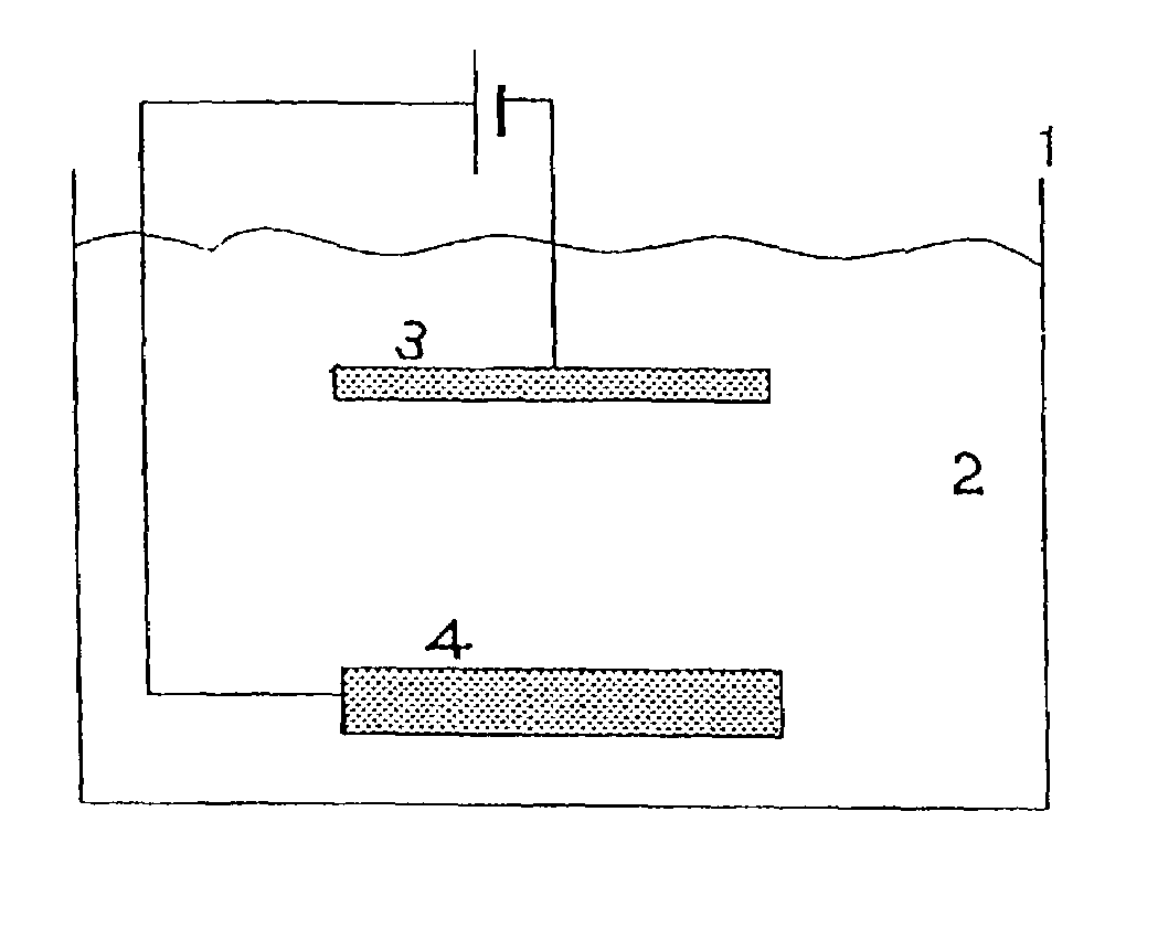
[0044]As shown in Table 1, phosphorous copper having a phosphorous content of 300 to 600 wtppm was used as the anode, and a semiconductor was used as the cathode. The crystal grain size of these phosphorous copper anodes was 10 to 200 μm.
[0045]As the plating liquid, copper sulfate: 20 to 55 g/L (Cu), sulfuric acid: 10 to 200 g/L, chlorine ion 60 mg/L, additive [brightening agent, surface active agent] (Product Name CC-1220: manufactured by Nikko Metal Plating): 1 mL/L were used. The purity of the copper sulfate within the plating liquid was 99.99%.
[0046]The plating conditions were plating temperature 30° C., cathode current density 1.0 to 5.0 A/dm2, anode current density 1.0 to 5.0 A/dm2, and plating time 19 to 96 hr. The foregoing conditions are shown in Table 1.
[0047]After the plating, the generation of particles and plate appearance were observed. The results are similarly shown in Table 1.
[0048]Regarding the particle amount, after having performed electrolysis under the foregoing electrolytic conditions, the plating liquid was filtered with a filter of 0.2 μm, and the weight of the filtrate was measured thereby.
[0049]Regarding the plate appearance, after having performed electrolysis under the foregoing electrolytic conditions, the object to be plated was exchanged, plating was conducted for 3 minutes, and the existence of burns, clouding, swelling, abnormal deposition, foreign material adhesion and so on were observed visually.
[0050]As a result of the foregoing experiments, the amount of particles was less than 1 mg in Examples 1 to 4, and the plate appearance was favorable.
Results Plate Appearance Favorable Favorable Favorable Favorable Regarding the particle amount, after having performed electrolysis under foregoing electrolytic conditions, the plating liquid was filtered with a filter of 0.2 μm, and the weight of the filtrate was measured thereby. Regarding the plate appearance, after having performed electrolysis under the foregoing electrolytic conditions, the object to be plated was exchanged, plating was conducted for 3 min., and the existence of burns, clouding, swelling, abnormal deposition, foreign material adhesion andso on were observed visually.
Example
Examples 5 to 8
[0052]As shown in Table 2, phosphorous copper having a phosphorous content of 500 wtppm was used as the anode, and a semiconductor was used as the cathode. The crystal grain size of these phosphorous copper anodes was 200 μm.
[0053]As the plating liquid, copper sulfate: 55 g/L (Cu), sulfuric acid: 10 g/L, chlorine ion 60 mg/L, additive [brightening agent, surface active agent] (Product Name CC-1220: manufactured by Nikko Metal Plating): 1 mL/L were used. The purity of the copper sulfate within the plating liquid was 99.99%.
[0054]The plating conditions were plating temperature 30° C., cathode current density 1.0 to 5.0 A/dm2, anode current density 1.0 to 5.0 A/dm2, and plating time 24 to 48 hr.
[0055]With the foregoing Examples 5 to 8, in particular, illustrated are examples in which minute crystal layers having a crystal grain size of 5 μm and 10 μm were previously formed on the anode surface at a thickness of 100 μm, and a black film was also formed thereon at a thickness of 100 μm and 200 μm.
[0056]The foregoing conditions are shown in Table 2.
[0057]After the plating, the generation of particles and plate appearance were observed. The results are similarly shown in Table 2. Moreover, the observation of the amount of particles and the plate appearance was pursuant to the same method as with Examples 1 to 4.
[0058]As a result of the foregoing experiments, the amount of particles was less than 1 mg in Examples 5 to 8, and the plate appearance was favorable.
[0059]Further, as shown in Table 2, in comparison to Examples 1 to 4, a prescribed plate was acquired in a short period of time with a relatively low current density. This is considered to be because minute crystal layers having a crystal grain size of 5 μm and 10 μm were previously formed on the anode surface at a thickness of 100 μm, and a black film was also formed thereon at a thickness of 100 μm and 200 μm.
[0060]Accordingly, it is evident that previously forming a minute crystal layer having a crystal grain diameter of 1 to 100 μm or a black film layer on the phosphorous copper anode surface is effective in forming a stable plate coating without any particles in a short period of time.
Results Plate Appearance Favorable Favorable Favorable Favorable Regarding the particle amount, after having performed electrolysis under the foregoing electrolytic conditions, the plating liquid was filtered with a filter of 0.2 μm, and the weight of the filtrate was measured thereby. Regarding the plate appearance, after having performed electrolysis under the foregoing electrolytic conditions, the object to be plated was exchanged, plating was conducted for 3 min., and the existence of burns, couding, cwelling, abnormal deposition, foreign material adhesionand so on were observed visually.
[0062]As shown in Table 3, phosphorous copper having a phosphorous content of 500 wtppm was used as the anode, and a semiconductor was used as the cathode. The crystal grain size of these phosphorous copper anodes was 3 μm and 2000 μm, which are both outside the scope of the present invention.
[0063]As the plating liquid, copper sulfate: 55 g/L (Cu), sulfuric acid: 10 g/L, chlorine ion 60 mg/L, additive [brightening agent, surface active agent] (Product Name CC-1220: manufactured by Nikko Metal Plating): 1 mL/L were used. The purity of the copper sulfate within the plating liquid was 99.99%.
[0064]The plating conditions were plating temperature 30° C., cathode current density 1.0 to 5.0 A/dm2, anode current density 1.0 to 5.0 A/dm2, and plating time 19 to 96 hr. The foregoing conditions are shown in Table 3.
[0065]After the plating, the generation of particles and plate appearance were observed. The results are similarly shown in Table 3.
[0066]Moreover, the observation of the amount of particles and the plate appearance was pursuant to the same method as with the foregoing Examples. As a result of the foregoing experiments, the amount of particles in Comparative Examples 1 to 3 reached 425 to 2633 mg, and the plate appearance was also unfavorable.
[0067]Accordingly, it has been confirmed that if the crystal grain size of the phosphorous copper anode is excessively large or small, the generation of particles will increase. Thus, it is evident that the optimization of the phosphorous copper anode is important.
[0068] TABLE 3 Comparative Examples 1 2 3 4 Anode Crystal Grain Size (μm) 3 2000 3 2000 Phosphorous Content (ppm) 500 500 500 500 Surface Layer — — — — Plating Liquid Metallic Salt Copper Sulfate: 55 g/ Copper Sulfate: 55 g/ Copper Sulfate: 55 g/ Copper Sulfate: 55 g/ L(Cu) L(Cu) L(Cu) L(Cu) Acid Sulfuric Acid: 10 g/L Sulfuric Acid: 10 g/L Sulfuric Acid: 10 g/L Sulfuric Acid: 10 g/L Chlorine Ion 60 60 60 60 Additive CC-1220: 1 mL/L CC-1220: 1 mL/L CC-1220: 1 mL/L CC-1220: 1 mL/L (Nikko Metal Plating) (Nikko Metal Plating) (Nikko Metal Plating) (Nikko Metal Plating) Electrolytic Bath Amount (mL) 700 700 700 700 Conditions Bath Temperature (° C.) 30 30 30 30 Cathode Semiconductor Wafer Semiconductor Wafer Semiconductor Wafer Semiconductor Wafer Cathode Area (dm2) 0.4 0.4 0.4 0.4 Anode Area (dm2) 0.4 0.4 0.4 0.4 Cathode Current Density (A/ 1.0 2.0 4.0 5.0 dm2) Anode Current Density (A/ 1.0 2.0 4.0 5.0 dm2) Time (h) 96 48 24 19 Evaluation Particle Amount (mg) 425 1522 758 2633 Results Plate Appearance Inferior Inferior Inferior Inferior Regarding the particle amount, after having performed electrolysis under the foregiong electrolytic conditions, the plating liquid filtered with a filter of 0.2 μm, and the weight of the filtrate was measured thereby. Regarding the plate appearance, after having performed electrolysis under the foregoing electrolytic conditions, the object to be plated was exchanged, plating was conducted for 3 min., and the existence of burns, clouding, swelling, abnormal deposition, foreign material adhesion andso on were observed visually.
[0069]The present invention yields a superior effect in that it is capable of suppressing the generation of particles such as sludge produced on the anode side within the plating bath, and capable of significantly preventing the adhesion of particles to a semiconductor wafer.
PUM
Property
Measurement
Unit
Grain size
10.0 ~ 1500.0
μm
Grain size
5.0 ~ 1500.0
μm
Grain size
1.0 ~ 100.0
μm
Description & Claims & Application Information
We can also present the details of the Description, Claims and Application information to help users get a comprehensive understanding of the technical details of the patent, such as background art, summary of invention, brief description of drawings, description of embodiments, and other original content. On the other hand, users can also determine the specific scope of protection of the technology through the list of claims; as well as understand the changes in the life cycle of the technology with the presentation of the patent timeline. Login to view more.