Method of transferring a laminate and method of manufacturing a semiconductor device

a technology of semiconductor devices and laminates, applied in the field of methods of transferring laminates and manufacturing methods, can solve the problems of difficult to make large-size glass and quartz substrates, heavy weight and easy breakage, and unsuitable thin-film transistor substrates

Inactive Publication Date: 2006-12-12
SEMICON ENERGY LAB CO LTD
View PDF23 Cites 155 Cited by
  • Summary
  • Abstract
  • Description
  • Claims
  • Application Information

AI Technical Summary

Benefits of technology

[0015]The present invention has been made in view of the above-mentioned problems, and an object of the present invention is to provide a method of bonding onto a transferring member an object to be peeled, which is peeled from a substrate in a short time without damage being imparted to the object to be peeled within a laminate.

Problems solved by technology

Glass and quartz are often used in thin film transistor substrates at present, and these substrates have disadvantages in that they are heavy and they easily break.
Further, it is difficult to make large-size glass and quartz substrates, and therefore they are unsuited to thin film transistor substrates from the viewpoint of mass production.
However, the present situation is that plastic has a low heat resistance, and therefore the maximum process temperature for forming the thin film transistors must be lowered.
As a result, thin film transistors cannot be formed having electrical characteristics that are as good as those of thin film transistors formed on substrates having relatively high heat resistance, such as glass substrates, and quartz substrates.
However, it is essential to use a substrate having good light transmitting characteristics with the methods disclosed in JP 10-125929 A and JP 10-125931 A, and therefore there is a problem in that the substrates capable of being used are limited.
Further, a relatively high-power laser light irradiation is necessary in order to impart an energy sufficient to pass through the substrate and cause hydrogen contained in the amorphous silicon to be emitted, and therefore there is a problem in that the laser light may damage the object to be peeled.
Further, if high-temperature heat treatment is performed in an element manufacturing process when manufacturing elements on the separation layer by the aforementioned methods, hydrogen contained in the separation layer diffuses and is reduced, and there is a concern that peeling cannot be sufficiently performed even if laser light is irradiated to the separation layer.
In addition, the transferring member is fixed to the surface of the object to be peeled using a curing adhesive, and therefore the surface of the object to be peeled, for example, the surface of the thin film transistor, specifically wirings or pixel electrodes are not exposed when peeling the substrate from the object to be peeled, and therefore it is difficult to measure the characteristics of the object to be peeled after peeling off the substrate.
For cases of manufacturing a liquid crystal display device or a light emitting device using an object to be peeled with this type of structure, the structure becomes one in which a plurality of substrates are bonded to one another, and the thickness of the liquid crystal display device or the light emitting device becomes larger, and there is a problem in that electronic devices cannot be made smaller when using the liquid crystal display device or the light emitting device.
Further, there is a problem in that projection light from a backlight in a liquid crystal display device, and light emitted from light emitting elements in a light emitting device each cannot be effectively taken out.
The object to be peeled and the second substrate are bonded by a water soluble adhesive in the invention disclosed in JP 2002-217391 A, but the surface area of the water soluble adhesive that is exposed to water is small in actuality, and therefore there is a problem in that peeling of the second substrate takes time.
The second substrate is disposable in this case, but there is a problem in that costs will increase when using expensive materials such as quartz glass, or rare materials in the second substrate.
In addition, if an organic resin is used in an interlayer insulating film of the thin film transistor, which is the object to be peeled, there is a problem in that the volume of the interlayer insulating film expands and the film deforms because organic resins tend to absorb moisture, and thin film transistor wirings will peel off.

Method used


Image

  • Method of transferring a laminate and method of manufacturing a semiconductor device
  • Method of transferring a laminate and method of manufacturing a semiconductor device
  • Method of transferring a laminate and method of manufacturing a semiconductor device

Examples


embodiment modes

[0044]Embodiment modes of the present invention are explained below.

embodiment mode 1

[Embodiment Mode 1]

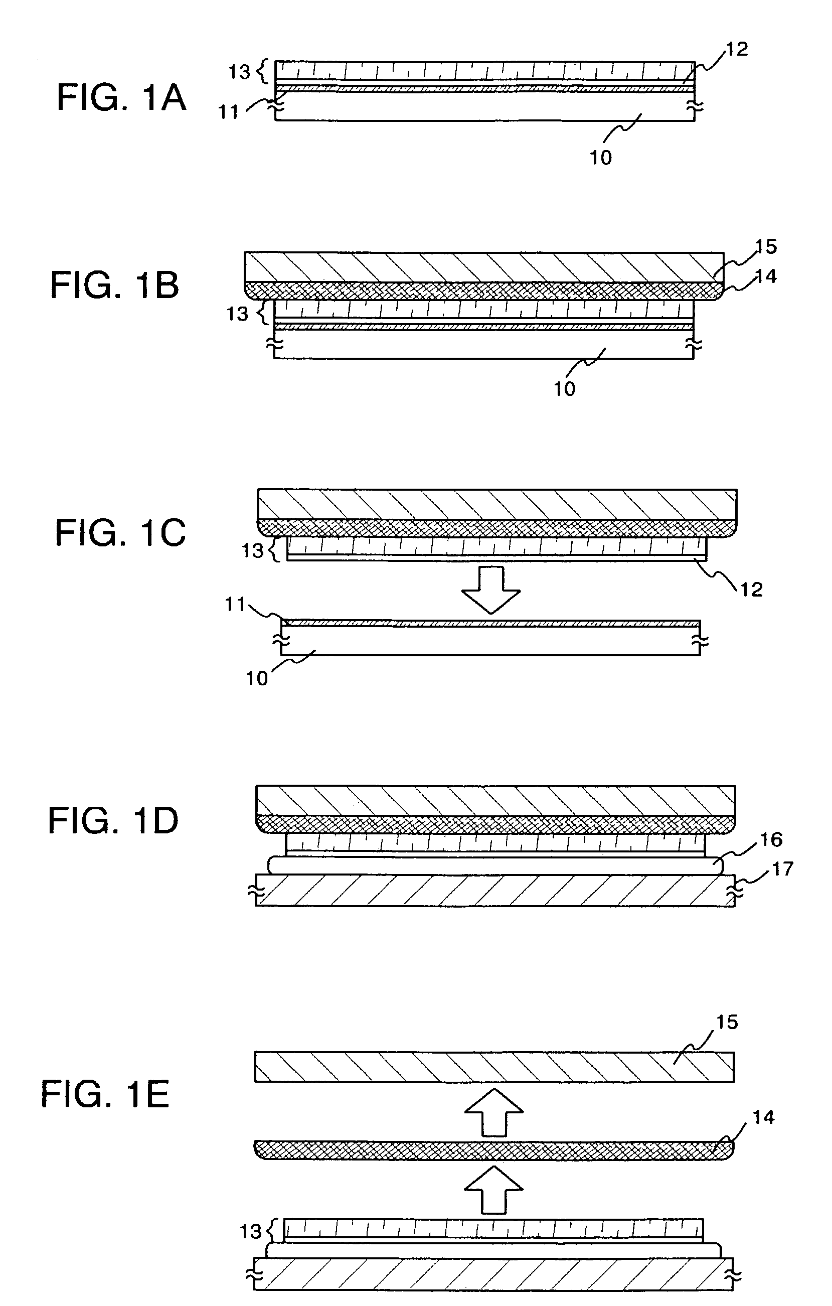
[0045]Procedures of a typical transferring method using the present invention are explained briefly using FIGS. 1A to 1E.

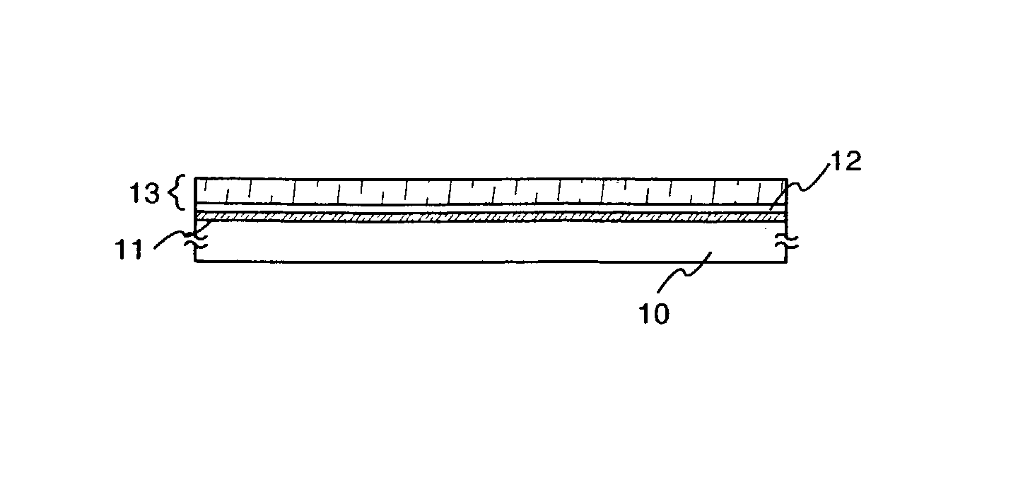
[0046]First, a description will be made with reference to FIG. 1A. Reference numeral 10 denotes a substrate, reference numeral 11 denotes a peeling layer, reference numeral 12 denotes an oxide layer, reference numeral 13 denotes an object to be peeled, and includes the oxide layer 12.

[0047]Glass substrates, quartz substrates, ceramic substrates, and the like can be used as the substrate 10. Further, silicon substrates, metallic substrates, and stainless steel substrates may also be used.

[0048]A peeling layer 11, which is a nitride layer or a metallic layer, is formed on the substrate 10. A typical example of the metallic layer includes a single layer made of an element selected from the group consisting of titanium (Ti), aluminum (Al), tantalum (Ta), tungsten (W), molybdenum (Mo), copper (Cu), chromium (Cr), neodymium (Ne), iron (Fe), nickel (Ni...

embodiment mode 2

[Embodiment Mode 2]

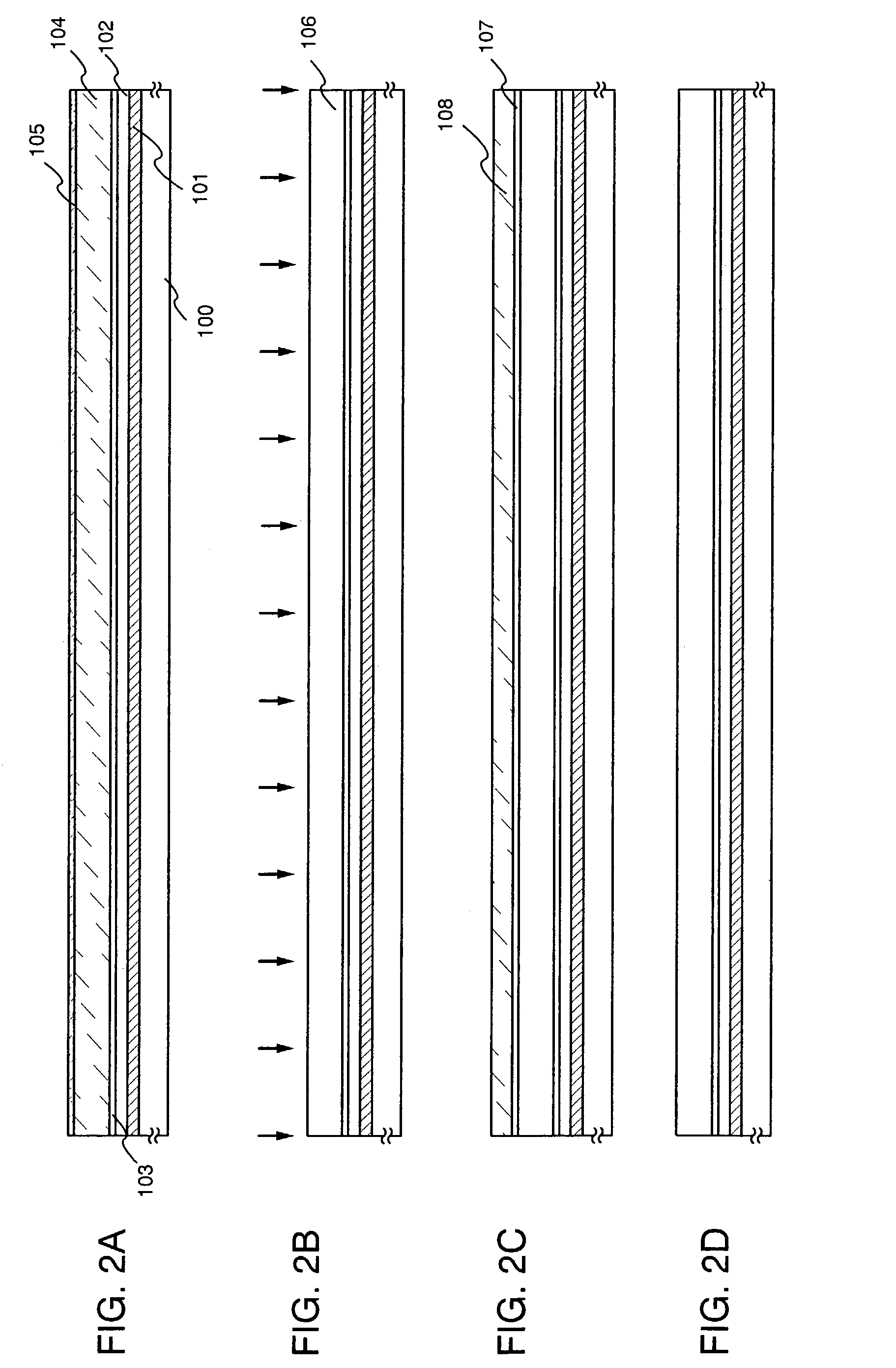
[0060]The structure of a peelable adhesive medium (two-sided tape is employed as a typical example) used in a transferring process of the present invention is explained here.

[0061]FIG. 11A and FIG. 11B are explained. The two-sided tape used in the present invention is one in which a first substrate 502 having a first adhesive 501, and a second substrate 504 having a second adhesive 503, are joined together by a cured adhesive 505. Heat-peeling adhesives and / or ultraviolet-peeling adhesives can be used in the first adhesive and in the second adhesive. Further, adhesives that are peelable by the irradiation of light (visible light, infrared light, and the like) (light peeling adhesives), and adhesives that are peelable by a chemical reaction (reaction peeling adhesives) can also be used as substitutes for the ultraviolet-peeling adhesives and the heat-peeling adhesives.

[0062]A heat-peeling adhesive and an ultraviolet-peeling adhesive are used as typical examples of ...


PUM

PropertyMeasurementUnit
period of timeaaaaaaaaaa
temperatureaaaaaaaaaa

Abstract

An object of the present invention is to provide a method of transferring an object to be peeled onto a transferring member in a short time without imparting damage to the object to be peeled within a laminate. Also, another object of the present invention is to provide a method of manufacturing a semiconductor device in which a semiconductor element manufactured on a substrate is transferred onto a transferring member, typically, a plastic substrate. The methods are characterized by including: forming a peeling layer and an object to be peeled on a substrate; bonding the object to be peeled and a support through a two-sided tape; peeling the object to be peeled from the peeling layer by using a physical method, and then bonding the object to be peeled onto a transferring member; and peeling the support and the two-sided tape from the object to be peeled.

Description

BACKGROUND OF THE INVENTION[0001]1. Field of the Invention[0002]The present invention relates to a method of transferring a laminate. In addition, the present invention relates to a method of manufacturing a semiconductor device having a circuit structured by semiconductor elements, typically thin film transistors, in which an object to be peeled that contains the semiconductor elements is transferred to a substrate. For example, the present invention relates to an electro-optical device, typically a liquid crystal module, a light emitting device, typically an EL module, or an electronic device in which such a device is mounted as parts thereof.[0003]2. Description of the Related Art[0004]In recent years the focus has been on techniques of structuring thin film transistors by using semiconductor layers (having a thickness on the order of several nm to several hundreds of nm) formed on a substrate having an insulating surface. The thin film transistors are widely employed in electron...

Claims


Application Information

Patent Timeline
Patent Type & Authority Patents(United States)
IPC IPC(8): B44C1/17B29C65/00H01B13/00H01L21/02B32B37/00B44C1/175H01B13/008H01L21/20H01L21/762
CPCH01L21/2007H01L21/76251Y10T428/14H01L2221/68368
Inventor TAKAYAMA, TORUGOTO, YUUGOMARUYAMA, JUNYAOHNO, YUMIKO
Owner SEMICON ENERGY LAB CO LTD
Why Eureka
Try Eureka