
System and method for imprint lithography to facilitate dual damascene integration in a single imprint act

a technology of imprint lithography and system, applied in the field of system and method of imprint lithography, can solve the problems of difficult to achieve small feature size and significant capital investment of optical equipment for traditional photolithographic processes

Active Publication Date: 2006-12-12
ADVANCED MICRO DEVICES INC
View PDF5 Cites 38 Cited by
  • Summary
  • Abstract
  • Description
  • Claims
  • Application Information

AI Technical Summary

Benefits of technology

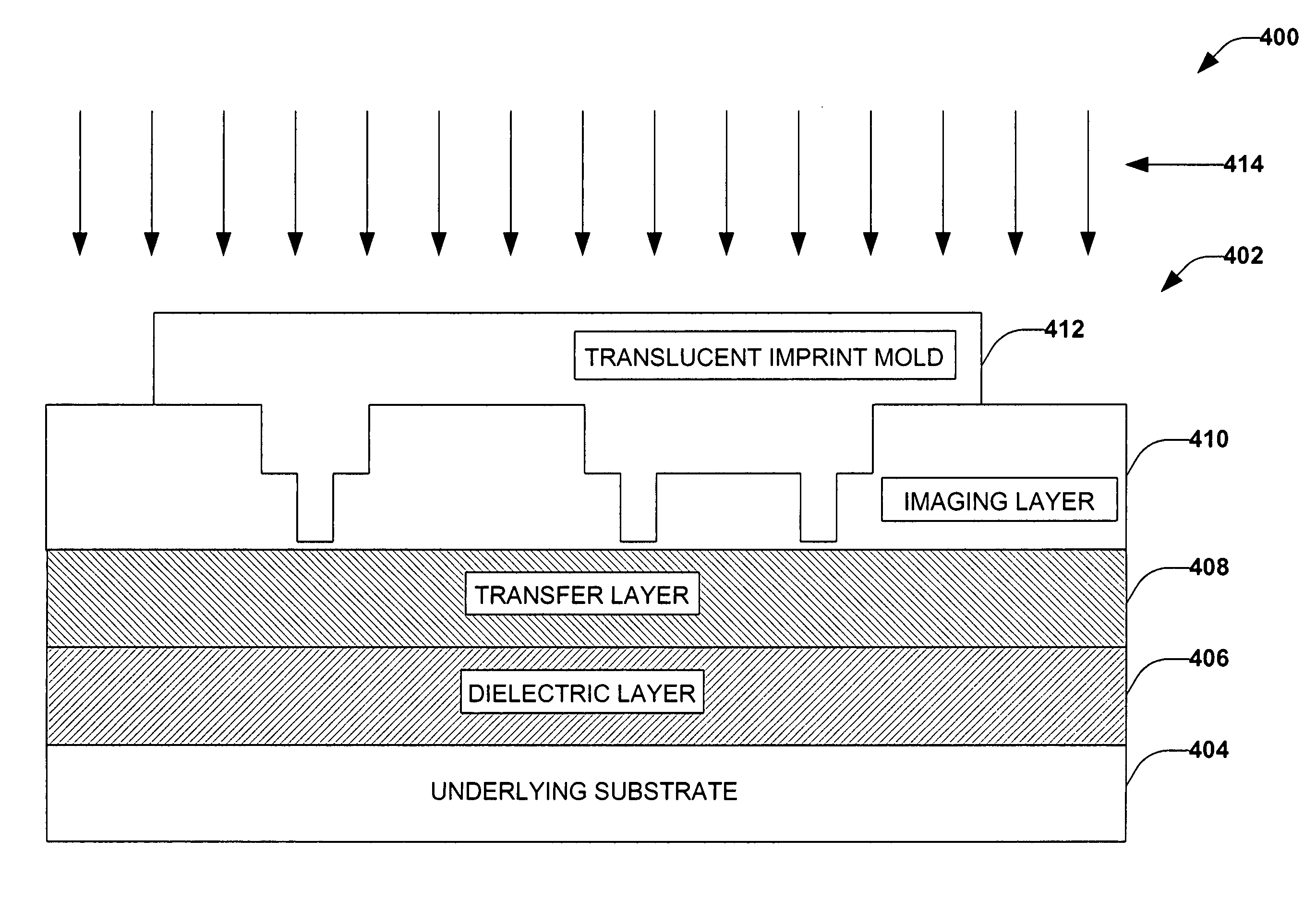
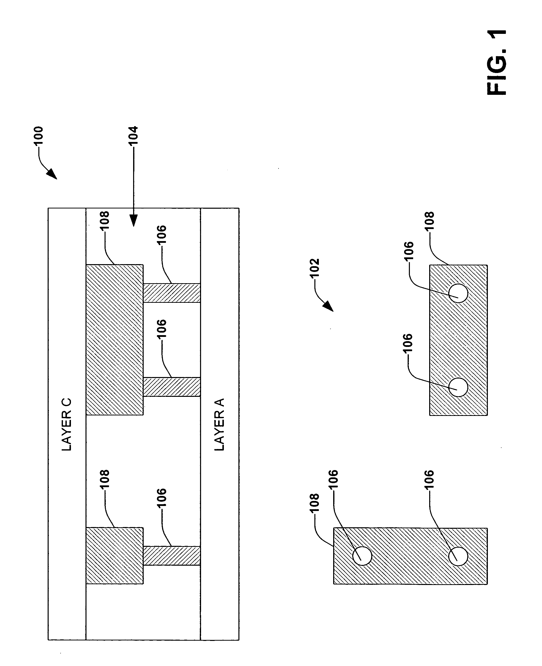
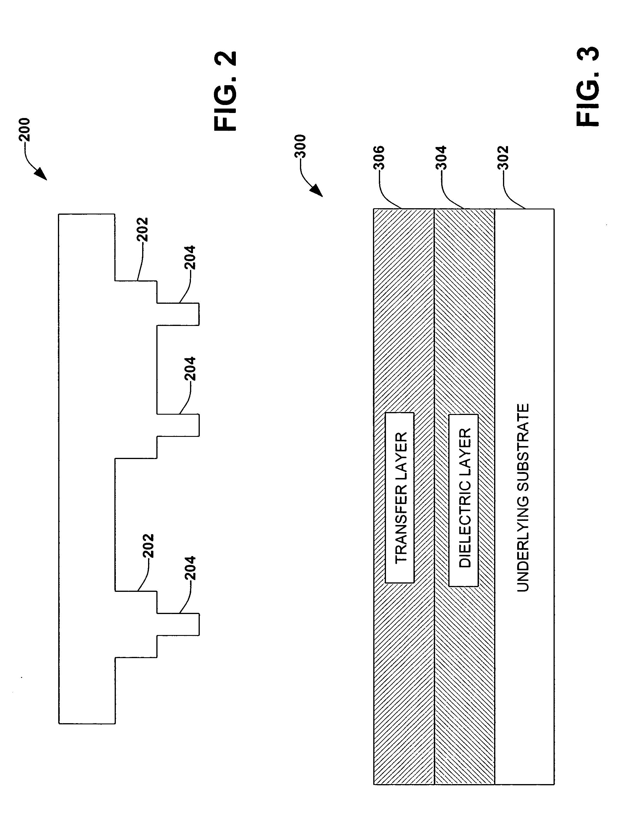
[0009]Systems and methods for imprint lithography are provided that facilitate the integration of dual damascene interconnect features in one imprint step. The present invention facilitates reproduction of features required for production of integrated circuits; specifically the invention provides for integration of dual damascene interconnect features (i.e. vias and trenches) in one imprint step. The present invention provides for creation of a translucent imprint mold with three-dimensional features comprising the desired dual damascene interconnect pattern. Once created, the dual damascene imprint mold is utilized to imprint the dual damascene pattern in a step and repeat fashion. In accordance with one aspect of the invention, scatterometry is used to generate observed optical signatures for comparison to known optical signatures to facilitate evaluation of the imprint mold for contamination and wear.
[0011]Once patterns have been imprinted in the imaging layer, they must be transferred through to the underlying transfer layer. In accordance with one aspect of the present invention, the dual damascene pattern is transferred into the transfer layer through a sequence of four plasma etches. Further, in accordance with this aspect of the present invention, the first and second etches effectively transfer the via portions of the dual damascene pattern from the imaging layer into the transfer layer and the third and fourth etches effectively transfer the trench portions of the dual damascene pattern from the imaging layer into the transfer layer. The first etch is a halogen breakthrough etch that anisotropically removes residual organosilicon in the imaging layer corresponding to the via features of the dual damascene pattern. This breakthrough etch “breaks through” the imaging layer and exposes portions of the underlying transfer layer. The second etch is an oxygen transfer etch, which utilizes the remaining organosilicon in the imaging layer as an etch mask to transfer the via portion of the dual damascene pattern into the underlying transfer layer. The silicon in the organosilicon imaging layer, and lack of silicon in the transfer layer, provide the needed etch selectivity between the imaging layer and the transfer layer.
[0012]The third etch is a second halogen breakthrough etch that anisotropically removes residual organosilicon in the imaging layer corresponding to the trench features of the dual damascene pattern, exposing corresponding portions of the underlying transfer layer. The fourth etch is a second oxygen transfer etch, which uses the remaining organosilicon in the imaging layer as an etch mask to transfer the trench features of the dual damascene pattern into the underlying transfer layer. Once again, the silicon in the organosilicon imaging layer, and lack of silicon in the transfer layer, provide the needed etch selectivity between the imaging layer and the transfer layer.
[0014]In accordance with yet another aspect of the present invention, the parameters of one or more etch processes may be altered based at least in part on the results of a comparison of an observed optical signature to a library of optical signatures. For example, if the observed optical signature corresponds to an insufficient depth of penetration into the transfer layer, the duration of the etch process as performed on succeeding devices is increased to allow for a deeper etch penetration. Similarly, if the observed optical signature corresponds to an over etch condition where the depth of penetration into the transfer layer is too deep, the duration of the etch process on succeeding devices is decreased to allow for a shallower etch penetration.

Problems solved by technology

The optical equipment for traditional photolithographic processes requires significant capital investment.
Because imprint lithographic methods do not utilize the typical 4×optical reduction employed in conventional lithographic processes, however, the small feature sizes are more difficult to achieve.

Method used


Image

  • System and method for imprint lithography to facilitate dual damascene integration in a single imprint act
  • System and method for imprint lithography to facilitate dual damascene integration in a single imprint act
  • System and method for imprint lithography to facilitate dual damascene integration in a single imprint act

Examples


Embodiment Construction

[0036]The present invention will now be described with reference to the drawings. The following detailed description is of the best mode presently contemplated by the inventors for practicing the invention. It should be understood that the description of these aspects are merely illustrative and that they should not be taken in a limiting sense.

[0037]As used in this application, the terms “mold”, “imprint mold”, and “imprint lithography mold” are used interchangeably to refer to an article comprising a three dimensional pattern used to imprint a pattern in deformable material utilized in the production of an integrated circuit. The terms “imprint lithography” and “nanoimprint lithography” are used interchangeably to describe a method of producing integrated circuits involving imprinting a pattern onto a resist and subsequent exposure by a source, typically ultraviolet light, to which the resist is reactive.

[0038]Furthermore, the term “component” as used in this application is intend...


PUM


Abstract

A system and method are provided to facilitate dual damascene interconnect integration in a single imprint step. The method provides for creation of a translucent imprint mold with three-dimensional features comprising the dual damascene pattern to be imprinted. The imprint mold is brought into contact with a photopolymerizable organosilicon imaging layer deposited upon a transfer layer which is spin coated or otherwise deposited upon a dielectric layer of a substrate. When the photopolymerizable layer is exposed to a source of illumination, it cures with a structure matching the dual damascene pattern of the imprint mold. A halogen breakthrough etch followed by oxygen transfer etch transfer the vias from the imaging layer into the transfer layer. A second halogen breakthrough etch followed by a second oxygen transfer etch transfer the trenches from the imaging layer into the transfer layer. A dielectric etch transfers the pattern from the transfer layer into the dielectric layer. A metal fill process then fills the dual damascene openings of the dielectric layer with metal.

Description

FIELD OF THE INVENTION[0001]The present invention generally relates to semiconductor processing and, more particularly, to systems and methods for imprint lithography that facilitate dual damascene interconnect integration in a single imprint step.BACKGROUND OF THE INVENTION[0002]In the semiconductor industry, there is a continuing trend toward higher device densities. To achieve these high densities there have been, and continue to be, efforts toward scaling down device dimensions (e.g., at sub-micron levels) on semiconductor wafers. In order to accomplish such high device packing densities, smaller and smaller feature sizes are required. This includes the width and spacing of interconnecting lines, spacing and diameter of contact holes, and the surface geometry, such as corners and edges, of various features. The dimensions of and between such small features can be referred to as critical dimensions. With an ever increasing number of integrated circuit features being formed on a c...

Claims


Application Information

Patent Timeline
IPC IPC(8): H01L21/44
CPCB82Y10/00B82Y40/00G03F7/0002H01L21/76807H01L21/76817H01L2221/1021
Inventor DAKSHINA-MURTHY, SRIKANTESWARASINGH, BHANWARPHAN, KHOI A.
Owner ADVANCED MICRO DEVICES INC
Learn More