Semiconductor device and manufacturing method thereof

a technology of semiconductor devices and manufacturing methods, applied in the direction of instruments, optics, transistors, etc., to achieve the effects of improving an operation characteristic and reliability of the semiconductor device, reducing manufacturing costs, and low consumption power

Inactive Publication Date: 2006-12-19
SEMICON ENERGY LAB CO LTD
View PDF55 Cites 59 Cited by
  • Summary
  • Abstract
  • Description
  • Claims
  • Application Information

AI Technical Summary

Benefits of technology

[0012]The present invention is a technique for solving the above problems, and an object of the present invention is to realize, in an electro-optical device and a semiconductor device which are represented by an active matrix liquid crystal display device manufa

Problems solved by technology

Thus, using one photomask means that processes such as resist peeling, washing, and drying, except for processes such as film formation and etching, are added before and aft

Method used


Image

  • Semiconductor device and manufacturing method thereof
  • Semiconductor device and manufacturing method thereof
  • Semiconductor device and manufacturing method thereof

Examples


embodiment 1

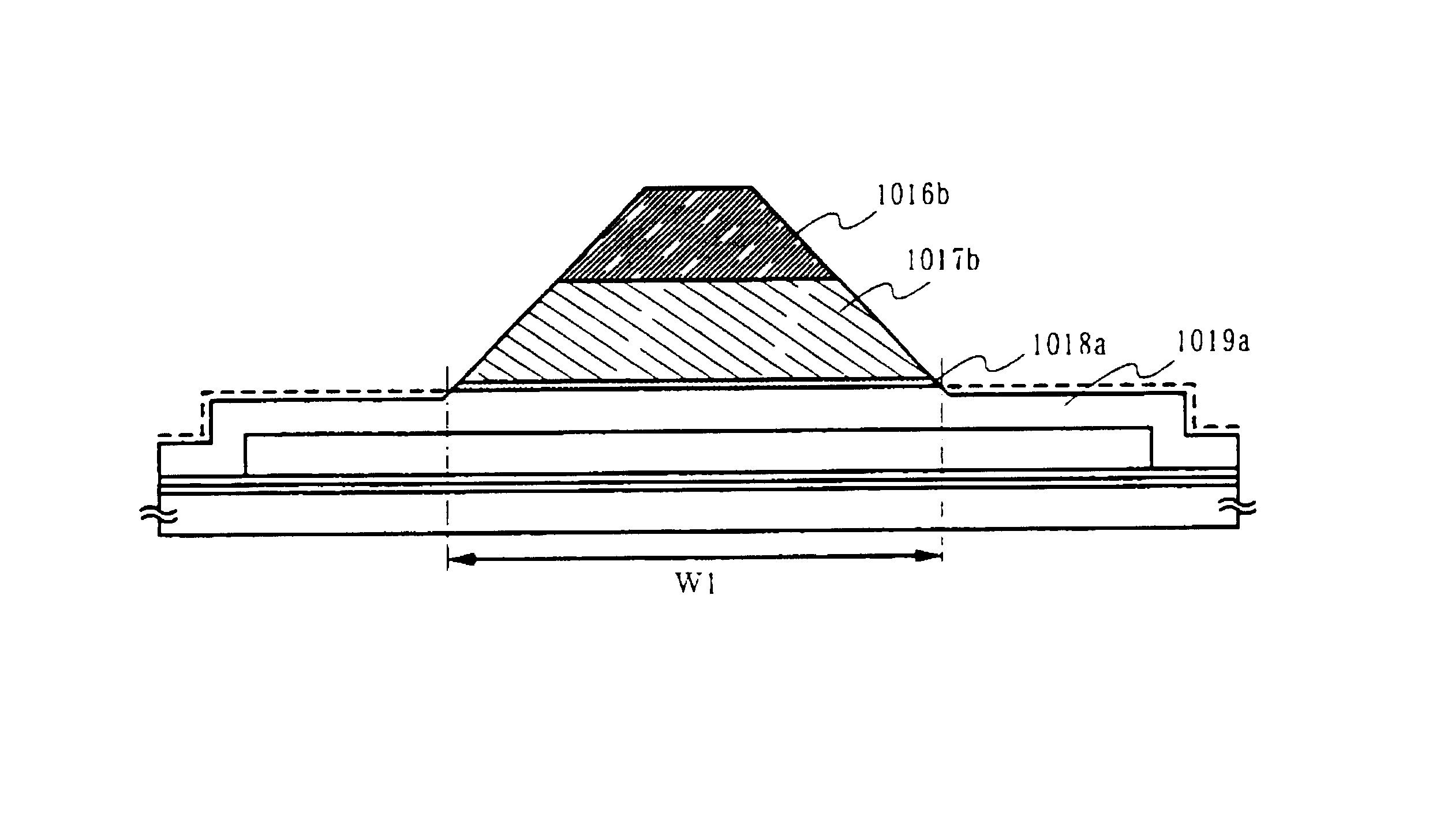
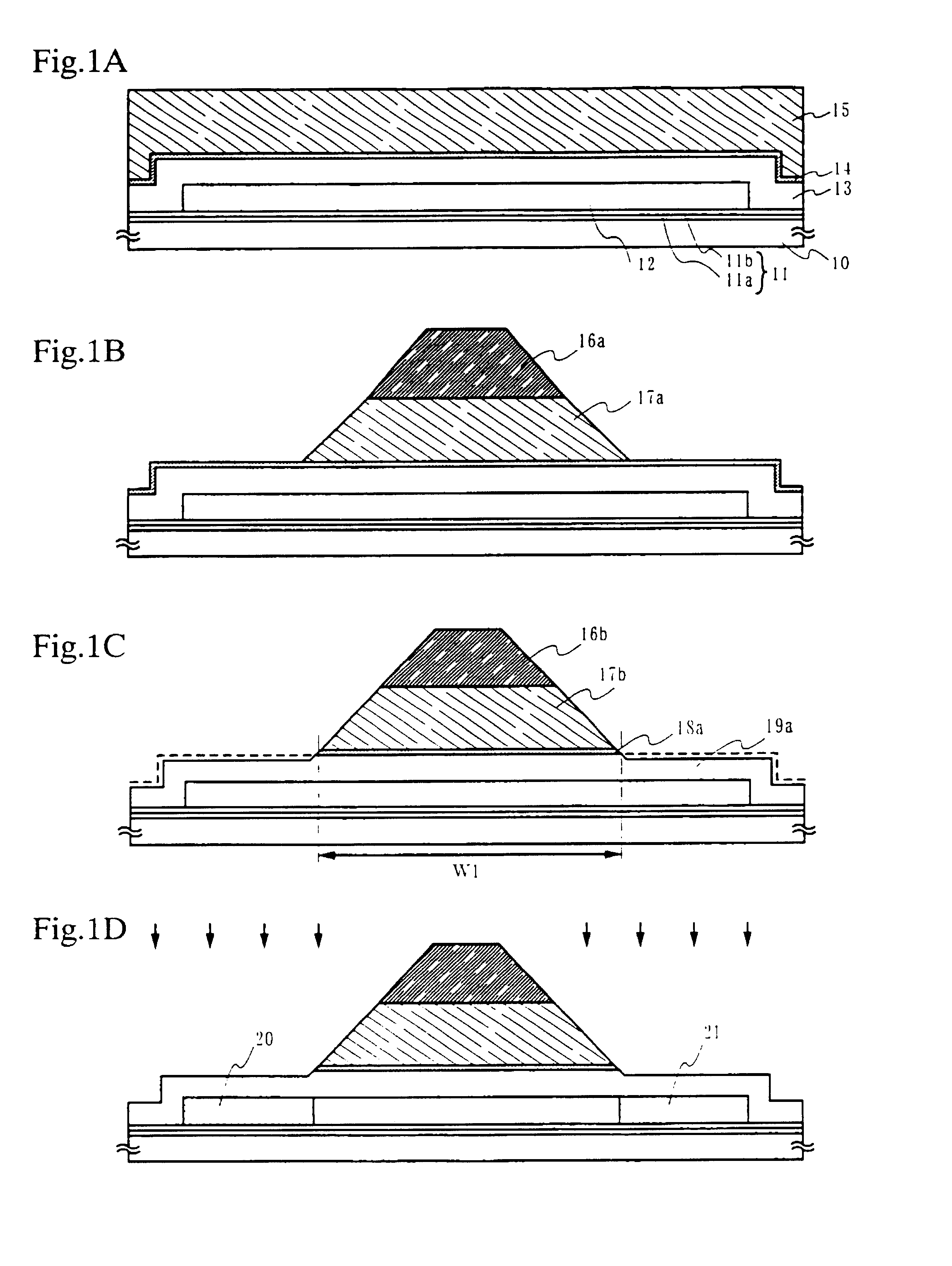
[0172]Here, a method of simultaneously forming, on the same substrate, a pixel portion and TFTs (n-channel TFT and p-channel TFT) of a driver circuit provided in the periphery of the pixel portion, is described in detail with FIGS. 7A to 9.

[0173]First, in this embodiment, a substrate 100 is used, which is made of glass such as barium borosilicate glass or aluminum borosilicate, represented by such as Corning #7059 glass and #1737 glass. Note that, as the substrate 100, there is no limitation provided that it is a substrate with transmittance, and a quartz substrate may be used. A plastic substrate with heat resistance to a process temperature of this embodiment may also be used.

[0174]Then, a base film 101 formed of an insulating film such as a silicon oxide film, a silicon nitride film or a silicon nitride oxide film is formed on the substrate 100. In this embodiment, a two-layer structure is used as the base film 101. However, a single-layer film or a lamination structure consistin...

embodiment 2

[0211]In this embodiment, a process for manufacturing an active matrix liquid crystal display device using the active matrix substrate manufactured in Embodiment 1 will be described. The description is made with reference to FIG. 10.

[0212]First, after the active matrix substrate with the state of FIG. 9 is obtained according to Embodiment 1, an orientation film 167 is formed on the active matrix substrate of FIG. 9 to perform a rubbing process. Note that, in this embodiment, before the formation of the orientation film 167, an organic resin film such as an acrylic resin film is patterned to form a columnar spacer for keeping a gap between substrates in a desired position. Also, instead of the columnar spacer, a spherical spacer may be distributed over the entire surface.

[0213]Next, a opposing substrate 168 is prepared. A color filter in which a colored layer 174 and a light shielding layer 175 are arranged corresponding to each pixel is provided in this opposing substrate 168. Also,...

embodiment 3

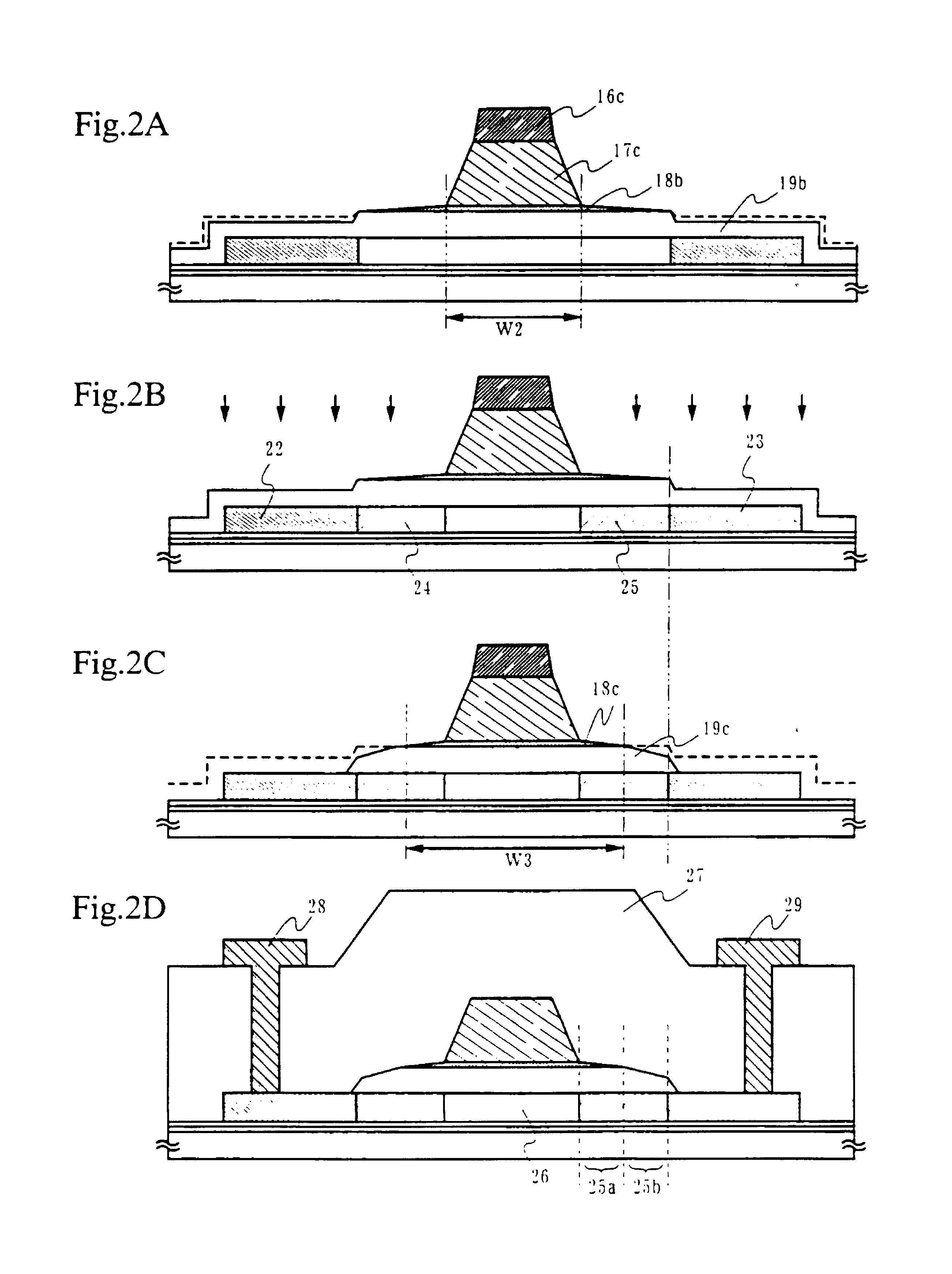
[0224]In this embodiment, a manufacturing method of an active matrix substrate different from that of Embodiment 1 will be described with reference to FIGS. 12A to 15, and FIGS. 17A and 17B. Although the transmission type display device is formed in Embodiment 1, in this embodiment, it is characterized in that a reflection type display device is formed to reduce the number of masks compared with Embodiment 1.

[0225]First, in this embodiment, a substrate 400 is used, which is made from glass, such as barium borosilicate glass or aluminum borosilicate glass, represented by Coming #7059 glass and #1737 glass. Note that, as the substrate 400, a quartz substrate, or a silicon substrate, a metal substrate, or a stainless substrate, on which an insulating film is formed, may be used as the replace. A plastic substrate having heat resistance to a process temperature of this embodiment may also be used.

[0226]Then, a base film 401 formed of an insulating film such as a silicon oxide film, a si...


PUM


Abstract

There has been a problem that the manufacturing process is complicated and the number of processes is increased when a TFT with an LDD structure or a TFT with a GOLD structure is formed. In a method of manufacturing a semiconductor device, after low concentration impurity regions (24, 25) are formed in a second doping process, a width of the low concentration impurity region which is overlapped with the third electrode (18c) and a width of the low concentration impurity region which is not overlapped with the third electrode can be freely controlled by a fourth etching process. Thus, in a region overlapped with the third electrode, a relaxation of electric field concentration is achieved and then a hot carrier injection can be prevented. And, in the region which is not overlapped with the third electrode, the off-current value can be suppressed.

Description

BACKGROUND OF THE INVENTION[0001]1. Field of the Invention[0002]The present invention relates to a semiconductor device comprising a circuit composed of thin film transistors (hereinafter referred to as TFTs) and a manufacturing method thereof, and for example, an electro-optical device which is represented by a liquid crystal display panel, an EL (electro luminescence) display device, an EC display device, and the like, and an electronic device in which such an electro-optical device is mounted as a part.[0003]Note that, in this specification, the semiconductor device represents all devices which can operate utilizing a semiconductor characteristic, and thus an electro-optical device, a semiconductor circuit, and an electronic device are all semiconductor devices.[0004]2. Description of the Related Art[0005]Recently, a development of a semiconductor device with a large area integrated circuit formed by a thin film transistor (TFT), which is formed using a semiconductor thin film (s...

Claims


Application Information

Patent Timeline
IPC IPC(8): H01L21/84H01L21/00H01L21/336H01L29/423H01L29/49H01L29/786
CPCH01L21/32136H01L27/1214H01L29/42384H01L29/4908H01L29/66757H01L29/78621H01L29/78627H01L29/78684H01L2029/7863H01L27/124H01L27/127H01L27/1288G02F1/134309G02F1/13439G02F1/1368
Inventor SUZAWA, HIDEOMIONO, KOJITAKAYAMA, TORUARAO, TATSUYAYAMAZAKI, SHUNPEI
Owner SEMICON ENERGY LAB CO LTD
Why Eureka
Try Eureka