Photovoltaic device and manufacturing method thereof

a photovoltaic device and manufacturing method technology, applied in the field of photovoltaic devices and photovoltaic devices manufacturing methods, to achieve the effect of reducing the average coordination number

Inactive Publication Date: 2007-01-16
SANYO ELECTRIC CO LTD
View PDF4 Cites 65 Cited by
  • Summary
  • Abstract
  • Description
  • Claims
  • Application Information

AI Technical Summary

Benefits of technology

[0015]According to the above mentioned structure, a network formed by covalent bonds of silicon atoms having a coordination number of four increases flexibility of the network structure by lacing atoms having a coordination number of two and belonging to group 6B of the periodic table. Therefore carrier recombination is suppressed while a defect density at the interface is reduced. As a result, open circuit voltage (Voc) and fill factor (F.F.) are improved
[0020]According to the above mentioned structure, a network formed by covalent bonds of silicon atoms having a coordination number of four increases flexibility of the network structure by lacing atoms having a coordination number of two and belonging to group 6B of the periodic table. Therefore a defect density at the interface is reduced.
[0023]Atoms, which reduce the average coordination number in the substantially intrinsic amorphous semiconductor thin film, exist in the interface formed with the crystalline semiconductor and the substantially intrinsic amorphous semiconductor thin film on the front surface side in a higher concentration than in a bulk.

Problems solved by technology

Therefore, excellent junction characteristics can be obtained even with an impure substrate, which is subject to an adverse effect of impurity or deficiency of oxygen induction under a high temperature process.

Method used


Image

  • Photovoltaic device and manufacturing method thereof
  • Photovoltaic device and manufacturing method thereof
  • Photovoltaic device and manufacturing method thereof

Examples


Embodiment Construction

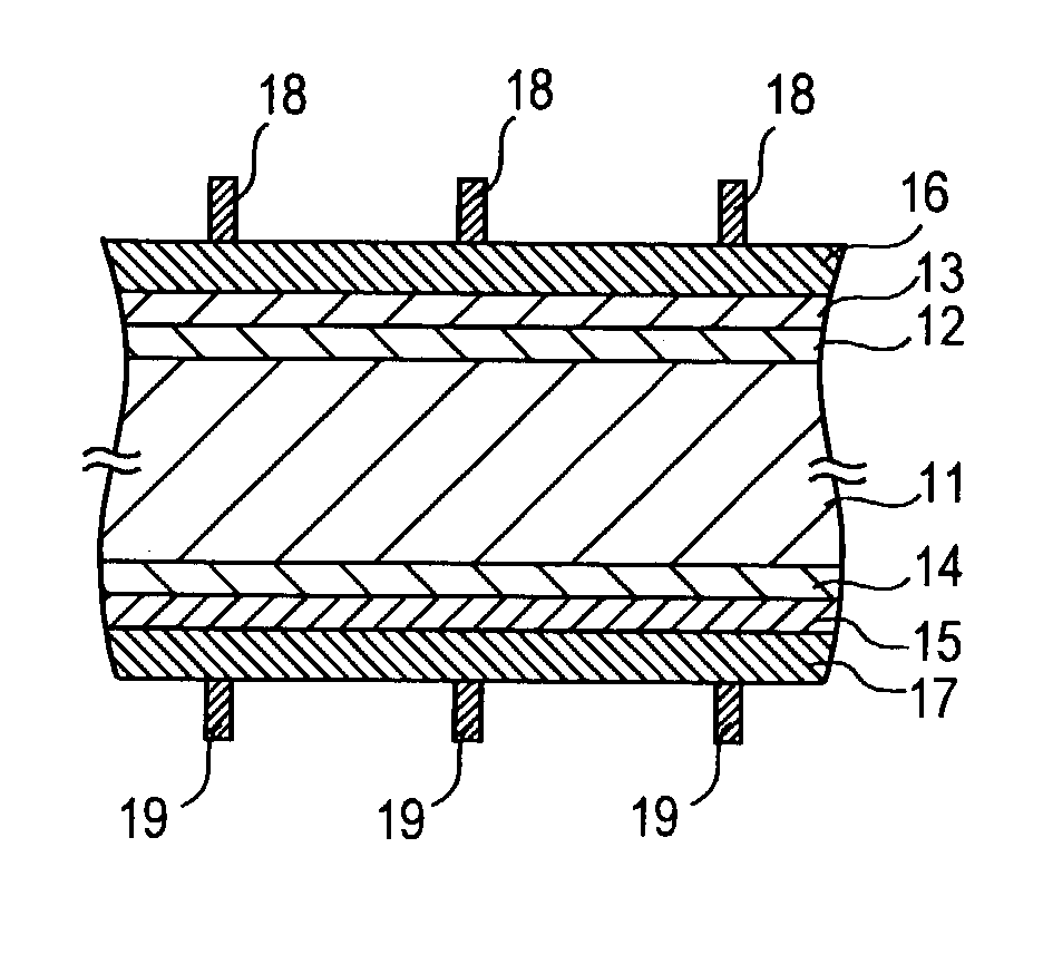
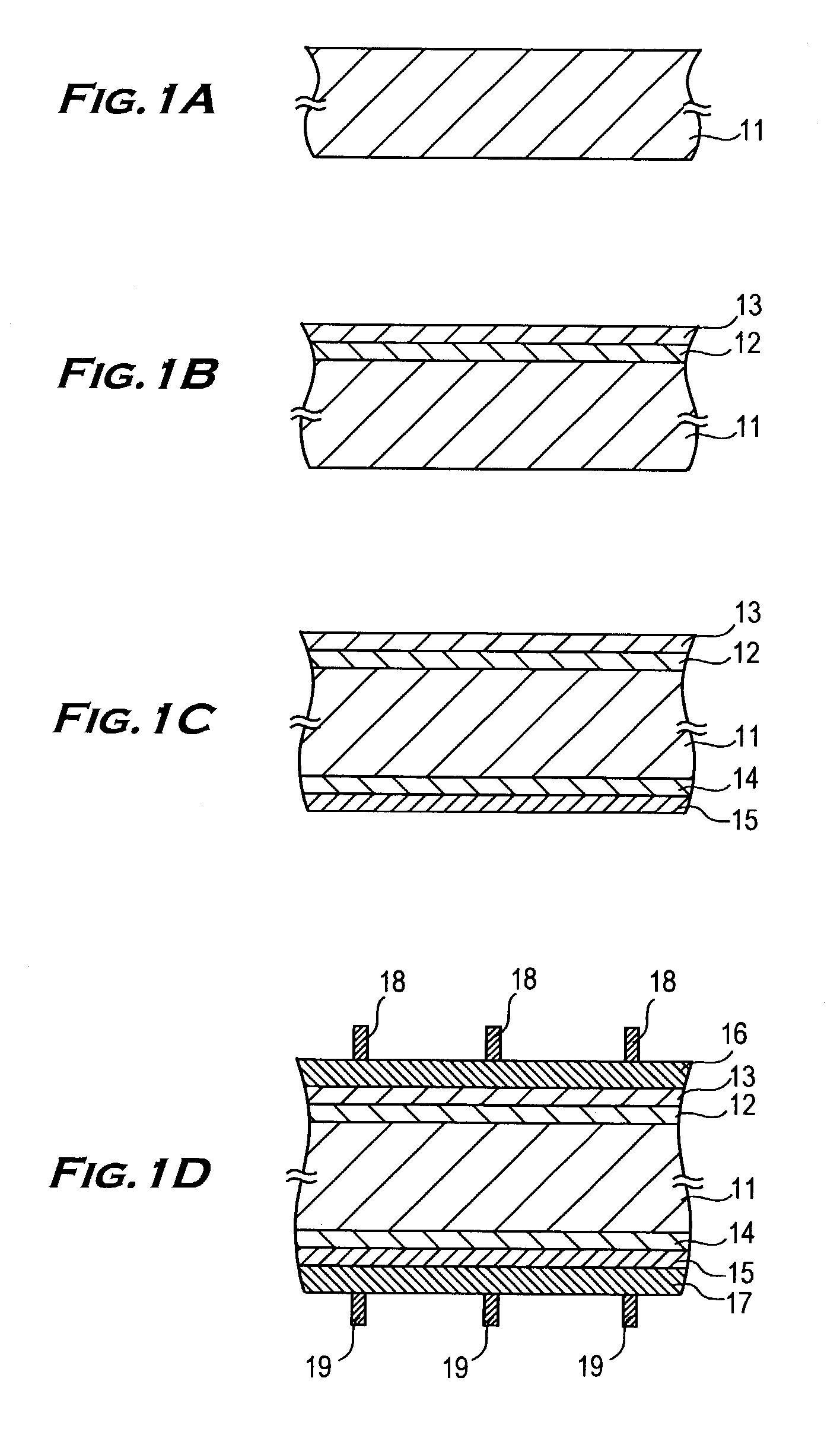
[0032]Following is a description on an embodiment of this invention with reference to drawings. FIGS. 1A to 1D are cross sectional views showing a photovoltaic device in each manufacturing process of the embodiment according to the invention.

[0033]A single crystalline silicon substrate, a polycrystalline silicon substrate or the like are used as a crystalline semiconductor substrate. In this embodiment, a single crystalline substrate 11 of resistivity not more than 5 Ωcm and 300 μm in thickness is employed. Both front and rear surfaces of this single crystalline silicon substrate 11 are textured by anisotropic etching using alkaline solution such as sodium hydroxide solution or potassium hydroxide solution.

[0034]The single crystalline silicon substrate 11 is cleaned and put into a vacuum chamber to be heated at temperatures up to 200° C., whereby the moisture on the substrate is almost removed. In this embodiment, the substrate is heated up to 170° C. Next, hydrogen gas (H2) is intr...


PUM

PropertyMeasurementUnit
temperatureaaaaaaaaaa
thicknessaaaaaaaaaa
resistivityaaaaaaaaaa

Abstract

In a photovoltaic device of the present invention, junction characteristics are improved by enhancing interface characteristics between a crystalline silicon semiconductor and an amorphous silicon semiconductor. In the photovoltaic device, an n-type crystalline substrate (11) and a p-type amorphous silicon thin film (13) are laminated with an i-type amorphous silicon thin film (12) interposed as well as an n-type amorphous silicon thin film (15) is provided on a rear surface of the crystalline silicon substrate (11) by interposing an i-type amorphous silicon thin film (14) between them. Oxygen atoms exist at interfaces between the crystalline silicon substrate (11) and the i-type amorphous silicon thin films (12), (14) in a higher concentration than that in the i-type amorphous silicon thin films (12), (14).

Description

BACKGROUND OF THE INVENTION[0001]1. Field of the Invention[0002]This invention relates to a photovoltaic device and a manufacturing method of the photovoltaic device.[0003]2. Description of Prior Art[0004]Photovoltaic devices are broadly categorized into single crystalline-, polycrystalline-, and amorphous-based type depending on a type of a semiconductor of a part for converting absorbed light into electric current. By taking advantage of features of the amorphous semiconductor thin film and crystalline semiconductor, a hybrid photovoltaic device with both types of semiconductor laminated has been researched. For example, U.S. Pat. No. 5,213,628 discloses a photovoltaic device of this kind. In this photovoltaic device, a substantially intrinsic amorphous silicon thin film is placed at a junction interface in forming semiconductor junction by combining a crystalline silicon semiconductor and an amorphous silicon semiconductor having different conductivity from each other so as to im...

Claims


Application Information

Patent Timeline
Patent Type & Authority Patents(United States)
IPC IPC(8): H01L29/04H01L31/20H01L31/0376H01L21/205H01L31/04H01L31/06H01L31/0747H01L31/075H01L31/077H01L31/18
CPCH01L31/03762H01L31/0747H01L31/202H01L31/077Y02E10/548Y02E10/547Y02P70/50
Inventor TERAKAWA, AKIRAASAUMI, TOSHIO
Owner SANYO ELECTRIC CO LTD
Why Eureka
Try Eureka