Method for fabricating semiconductor device

a semiconductor and fabrication method technology, applied in the direction of semiconductor devices, electrical devices, transistors, etc., can solve the problems of excessive etching of silicon film, excessive etching inability to increase the etching rate of titanium fluoride and titanium oxide, so as to reduce the number of grain boundaries formed

Active Publication Date: 2007-01-23
PANNOVA SEMIC
View PDF16 Cites 11 Cited by
  • Summary
  • Abstract
  • Description
  • Claims
  • Application Information

AI Technical Summary

Benefits of technology

[0063]Thus, even in the case where the concentration of a group V impurity in the silicon film is higher than the solubility limit in the silicon film, damage such as punch-through of the gate insulating film starting from a grain boundary of the silicon film can be prevented. This is because, since the temperature of heat applied from implantation of the group V impurity to etching of the polymetal structure is lower than 550° C., the amorphous silicon film is not polycrystallized, so as to reduce the number of grain boundaries formed in the silicon film.

Problems solved by technology

However, when the anisotropic etching for forming the n-type and p-type polymetal gate electrodes 23 and 24 is carried out as described above, there arises a problem that punch-through is locally caused in the gate insulating film 11 formed below the n-type polysilicon film 15.
Accordingly, the etching rates of the titanium fluoride and the titanium oxide cannot be increased.
In conclusion, the causes of the punch-through of the gate insulating film are: (1) since the concentration of the group V impurity in the silicon film exceeds the solubility limit, the silicon film is excessively etched in its grain boundary in the procedure for removing the residue of the barrier film of a tungsten nitride film or a titanium nitride film and the natural oxide film present on the silicon film; and (2) when the barrier film is made of a titanium nitride film, the silicon film is excessively etched in the procedure for removing the residue of the titanium nitride film or the natural oxide film present on the silicon film.

Method used


Image

  • Method for fabricating semiconductor device
  • Method for fabricating semiconductor device
  • Method for fabricating semiconductor device

Examples


embodiment 1

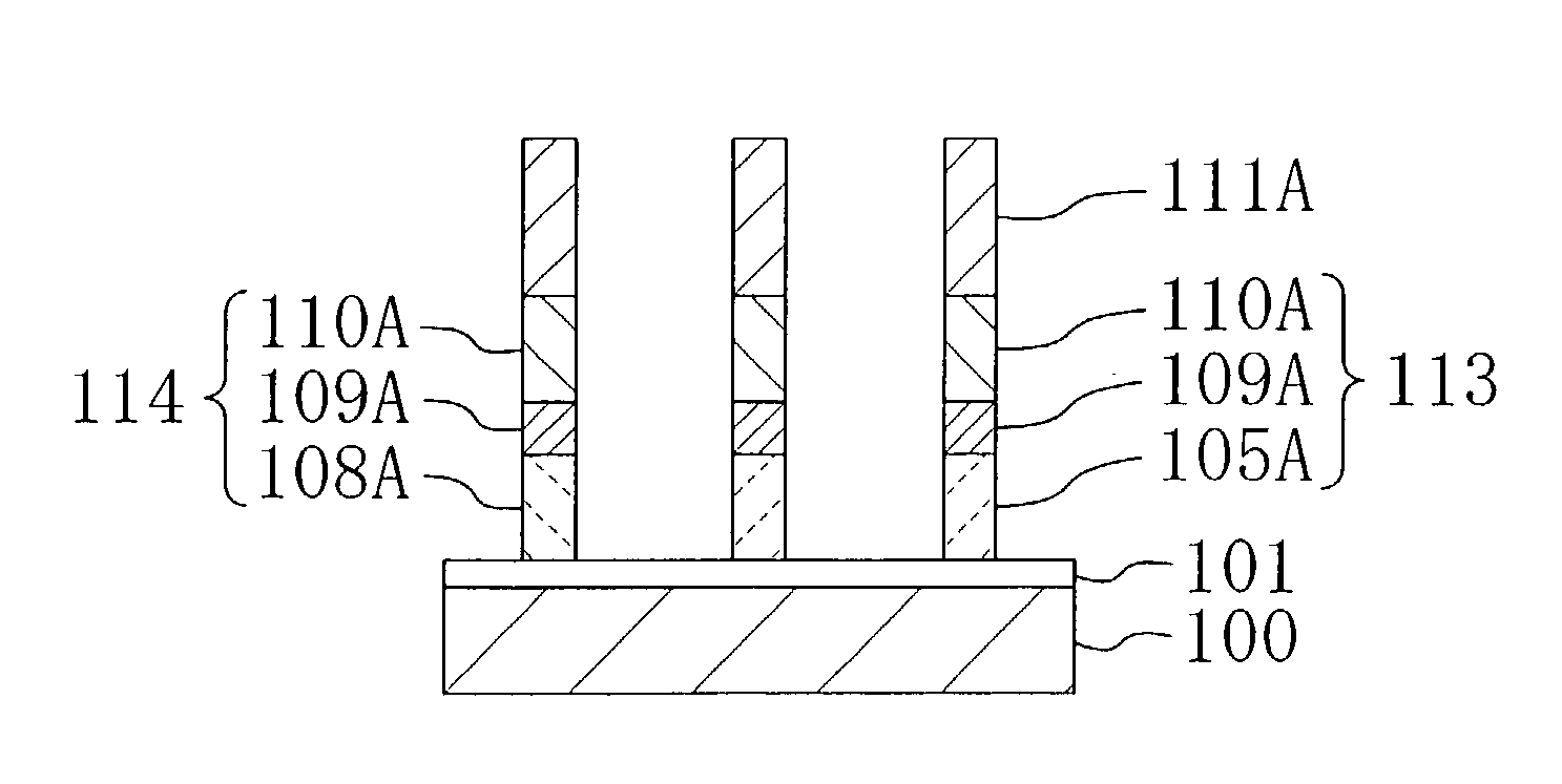
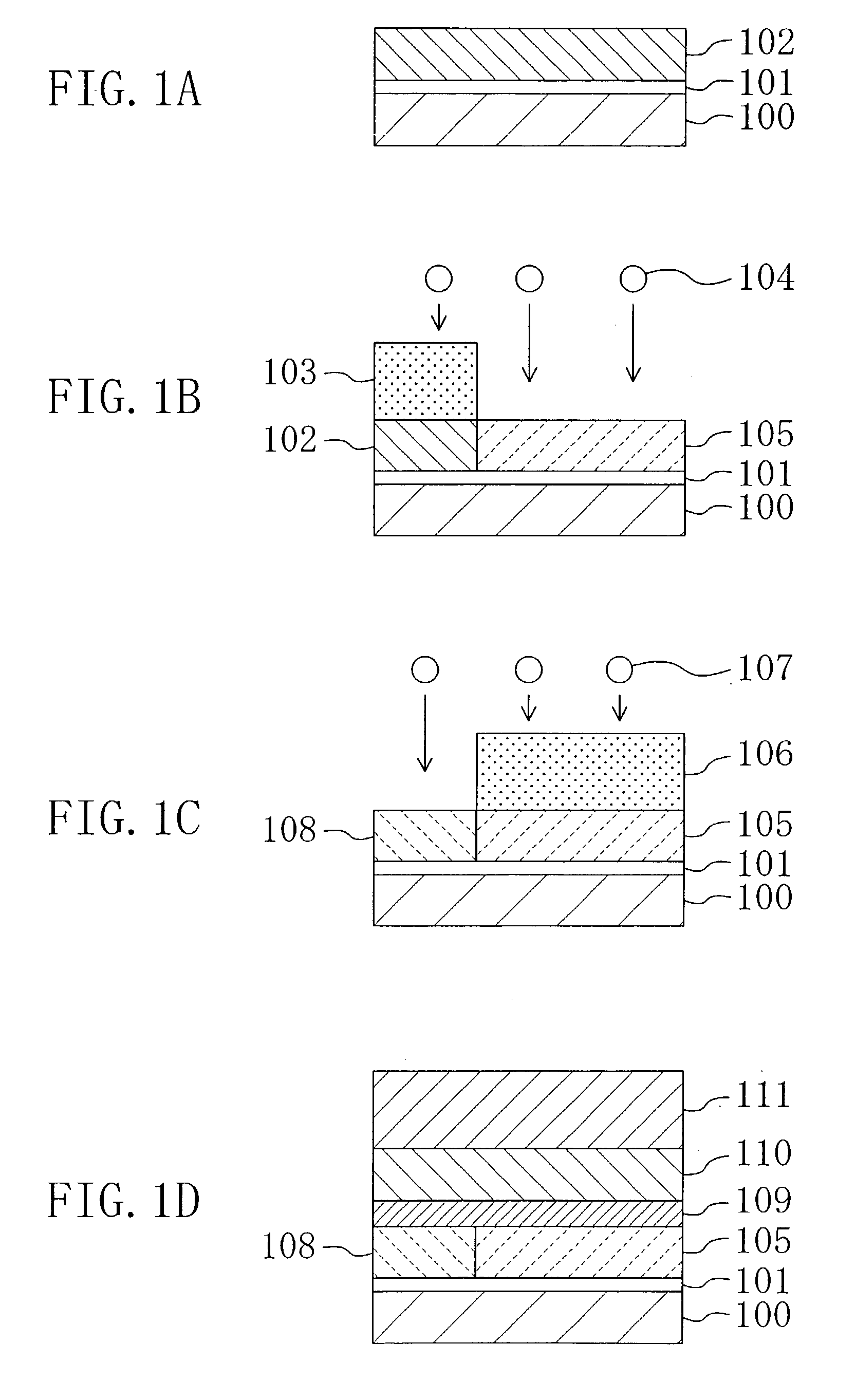
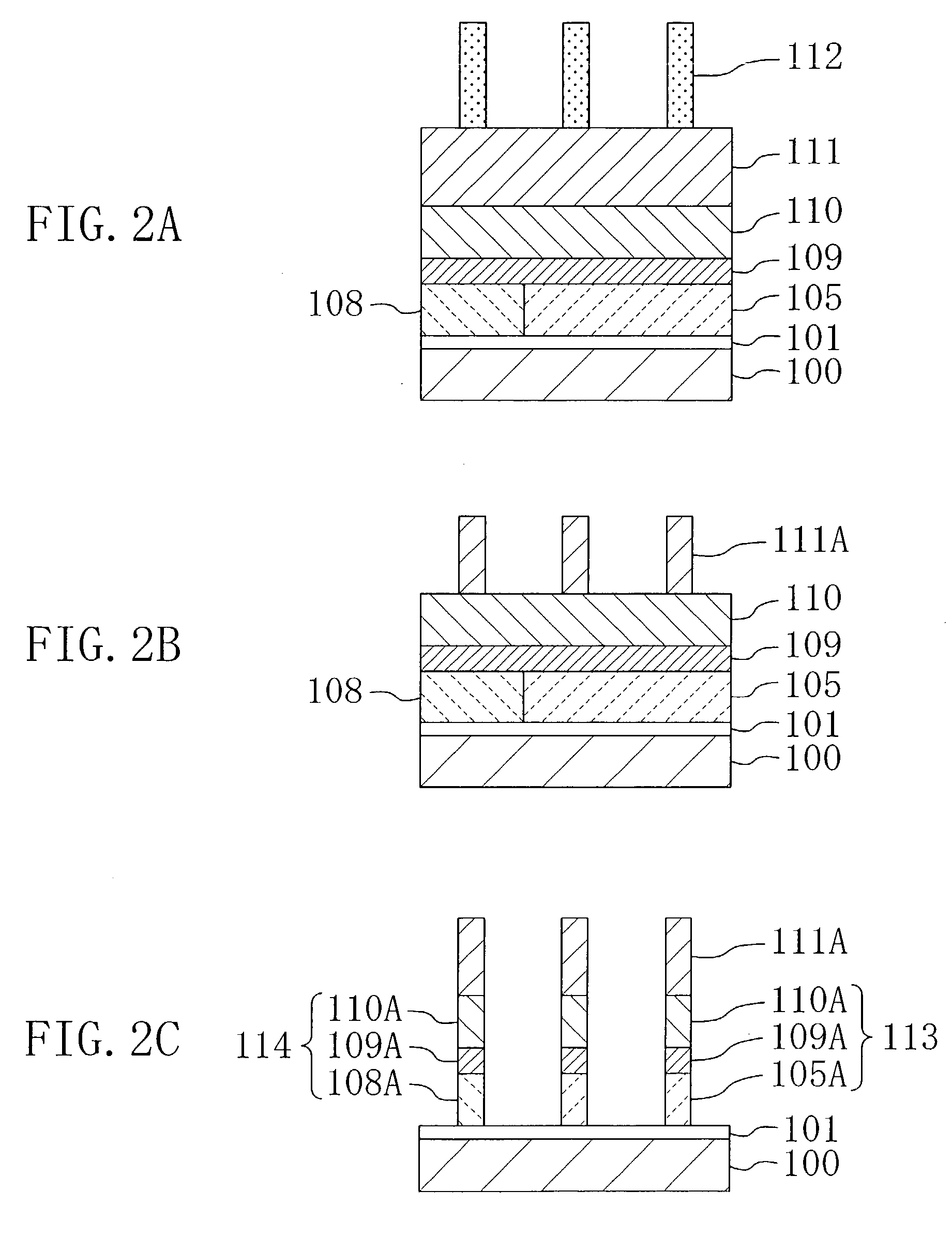
[0078]A method for fabricating a semiconductor device according to Embodiment 1 of the invention will now be described with reference to FIGS. 1A through 1D and 2A through 2C. In Embodiment 1, an implanted impurity is prevented from depositing in a grain boundary of a silicon film of a polymetal structure.

[0079]First, as shown in FIG. 1A, a gate insulating film 101 of a silicon oxide film with a thickness of, for example, 3 nm is formed on a semiconductor substrate 100 of silicon or the like by, for example, thermal oxidation. Thereafter, a polysilicon film 102 with a thickness of, for example, 100 nm is deposited on the gate insulating film 101 by, for example, CVD.

[0080]Next, as shown in FIG. 1B, after forming a first resist pattern 103 in a first predetermined portion on the polysilicon film 102, a group V impurity 104 of phosphorus (P) or the like is implanted into the polysilicon film 102 by ion implantation at a dose of, for example, 5×10¹⁴ / cm2, so as to form an n-type polysil...

embodiment 2

[0127]A method for fabricating a semiconductor device according to Embodiment 2 of the invention will now be described. As a characteristic of Embodiment 2, in the case where a group V impurity is deposited in a grain boundary of a polysilicon film included in a polymetal structure, chlorine is included in an etching gas used for removing a residue of a barrier film and a natural oxide film present on the polysilicon film. The conditions for the etching of a tungsten film 110 and a tungsten nitride film 109 and the conditions for the main etching and the over-etching of an n-type polysilicon film 105 and a p-type polysilicon film 108 are the same as those employed in Embodiment 1. Accordingly, three conditions for removing the residue and the natural oxide film alone will be herein described.

[0128](1) First conditions employed when the etching gas is a mixed gas of Cl2 and HBr:

[0129]Pressure: 0.4 Pa

[0130]First RF power: 400 W (13.56 MHz)

[0131]Second RF power: 60 W (13.56 MHz)

[0132]F...

embodiment 3

[0162]A method for fabricating a semiconductor device according to Embodiment 3 of the invention will now be described. As a characteristic of Embodiment 3, in the case where a group V impurity is deposited in a grain boundary of a polysilicon film included in a polymetal structure, an etching gas used for removing a residue of a barrier film and a natural oxide film present on the polysilicon film is a mixed gas of a gas including chlorine and a fluorocarbon gas. The conditions for the etching of a tungsten film 110 and a tungsten nitride film 109 and the conditions for the main etching and the over-etching of an n-type polysilicon film 105 and a p-type polysilicon film 108 are the same as those employed in Embodiment 1. Accordingly, conditions for removing the residue and the natural oxide film alone will be herein described. In this embodiment, a Cl2 gas is used as the gas including chlorine, and a CF4 gas is used as the fluorocarbon gas.

[0163](1) Conditions for removing residue ...


PUM

PropertyMeasurementUnit
temperatureaaaaaaaaaa
widthaaaaaaaaaa
thicknessaaaaaaaaaa

Abstract

After forming a gate insulating film on a semiconductor substrate, a silicon film is deposited on the gate insulating film, and a high-melting point metal film is deposited on the silicon film. After forming a hard mask made of a silicon oxide film or a silicon nitride film on the high-melting point metal film, the high-melting point metal film is dry etched by using the hard mask as a mask. After removing a residue or a natural oxide film present on the silicon film through dry etching, the silicon film is dry etched by using the hard mask as a mask. The residue or the natural oxide film is removed while suppressing excessive etching of the silicon film.

Description

BACKGROUND OF THE INVENTION[0001]The present invention relates to a method for fabricating a semiconductor device including a polymetal gate electrode made of a multilayer structure composed of a silicon film, a barrier film and a high-melting point metal film.[0002]Recently, the performance of semiconductor devices has been remarkably improved, and there are increasing demands for a higher operation speed and lower power consumption of semiconductor devices. For example, in a fine semiconductor device having a gate width of 0.15 μm or less, for further improvement of the performance of transistors, heteropolar electrodes, that is, a p+-type electrode used for a P channel transistor and an n+-type electrode used for an N channel transistor, have been started to be used as gate electrodes instead of conventionally used n+-type homopolar electrodes.[0003]Also, in order to further increase the operation speed and further reduce the power consumption of a semiconductor device, it is nec...

Claims


Application Information

Patent Timeline
Patent Type & Authority Patents(United States)
IPC IPC(8): H01L21/302H01L21/28H01L21/3065H01L21/3213H01L21/8238H01L27/092H01L29/423H01L29/49H01L29/78
CPCH01L21/32137H01L21/32136
Inventor DOSHITA, HIDEKI
Owner PANNOVA SEMIC
Why Eureka
Try Eureka