Deflectable microstructure and method of manufacturing the same through bonding of wafers

a microstructure and wafer technology, applied in microstructural technology, microstructure devices, microstructure devices, etc., can solve the problems of incompatibility or less than ideal for certain applications of each bonding technique, optical inefficiency and non-uniformity, and high voltage addressing of pixels, so as to achieve the effect of improving the spacing accuracy

Inactive Publication Date: 2007-02-06
SILEX MICROSYST
View PDF30 Cites 21 Cited by
  • Summary
  • Abstract
  • Description
  • Claims
  • Application Information

AI Technical Summary

Benefits of technology

[0014]In another embodiment the spacing accuracy is further improved by employing spacing elements.
[0021]excellent reflective properties, operable with wave lengths down to about 100 nm (deposition of different materials, e.g metals such as gold increases the reflectivity for longer wave lengths 600–2000 nm);

Problems solved by technology

The known beam SLMs have problems including beam insulator charging effects, lack of overvoltage protection against beam collapse, small-angle and nonuniform beam deflection leading to optical inefficiency and nonuniformity, and high voltage addressing of the pixels.
As can be expected, each of these bonding techniques can be incompatible or less than ideal for certain applications.
Silicon direct and anodic bonding methods require very smooth bonding surfaces, and therefore cannot produce a vacuum seal when unplanarized metal crossunders are employed, as is often required to electrically interconnect resonating and tunneling micromachines to bond pads outside the vacuum-sealed cavity of a sensor.
However, organic adhesives have not been found to reliably seal micromachines under vacuum, and bonding techniques employing glass frit require temperatures typically in the range of about 385° C. to 410° C., which can cause polysilicon, electroformed metal and LIGA micromachines to warp, bend and / or become electrically unstable.
As a further example, yaw sensors with resonating micromachined structures are prone to exhibit zero offset drift, compass effect and start-up drift if subjected to the temperatures necessary to bond wafers with glass frit.
A drawback to this requirement is the close alignment tolerances required to align the solderable rings, which complicates the bonding process when performed in a vacuum to obtain an evacuated cavity for housing the micromachine.
However, there are still some problems, i.a. the Al mirrors are made by deposition processes and are not mono crystalline, and therefore they cannot be perfectly planar, neither on a microscale nor on a macroscale.
Furthermore, they all suffer from hysteresis effects to some extent.

Method used


Image

  • Deflectable microstructure and method of manufacturing the same through bonding of wafers
  • Deflectable microstructure and method of manufacturing the same through bonding of wafers
  • Deflectable microstructure and method of manufacturing the same through bonding of wafers

Examples


embodiment 3

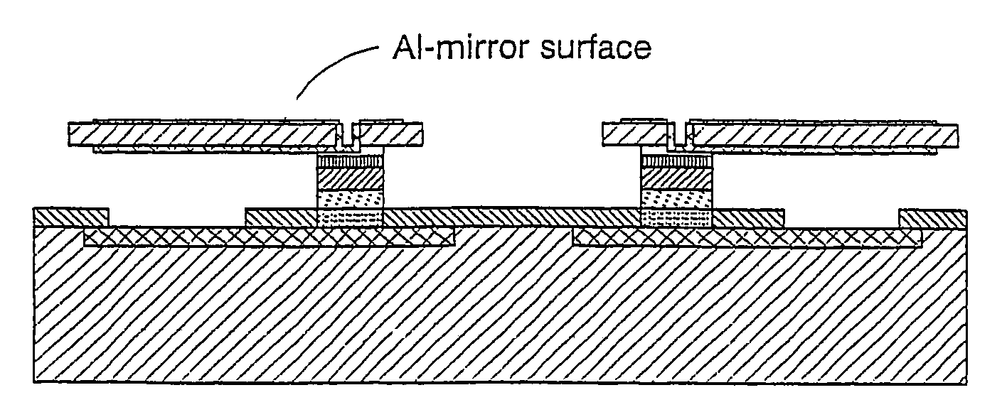
[0077]FIG. 8 schematically shows a third preferred embodiment of the final mirror or mirror arrays device fabricated according to the invention.,

[0078]In summary the process can be described as follows with reference to FIGS. 6–7:

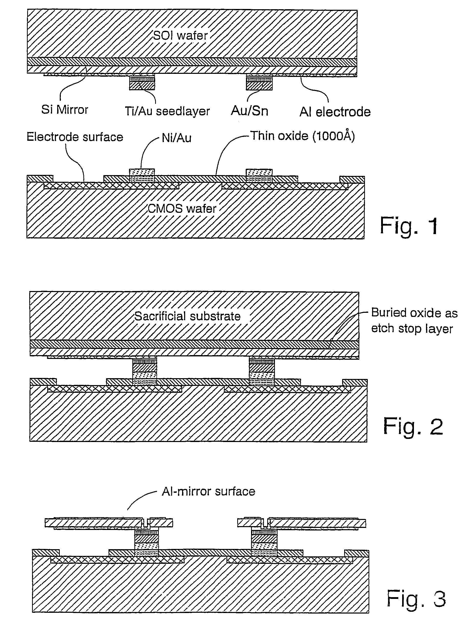
[0079]Making the SOI-wafer (Top-wafer) which is then normally is not processed further before the AuSi eutectic bonding. Optionally this wafer can be deposited with a metal layer as mirror electrodes following the processing according to embodiment 1.

[0080]The second wafer (bottom wafer in FIG. 6), which can be a CMOS wafer or a plain Si wafer structured or non-structured, comprises electrodes made by depositing suitable electrically conductive materials such as Al, Au, Ni, Ti etc or using highly doped silicon as it is or using a plain or structured wafer with wafer through vias (i.e. electrical connections through the wafer). The bottom wafer is also provided with eutectic bumps (as defined above) of e.g. Ni / Au or TiW / Au, consisting of a diffusion barrier ...

embodiment 4

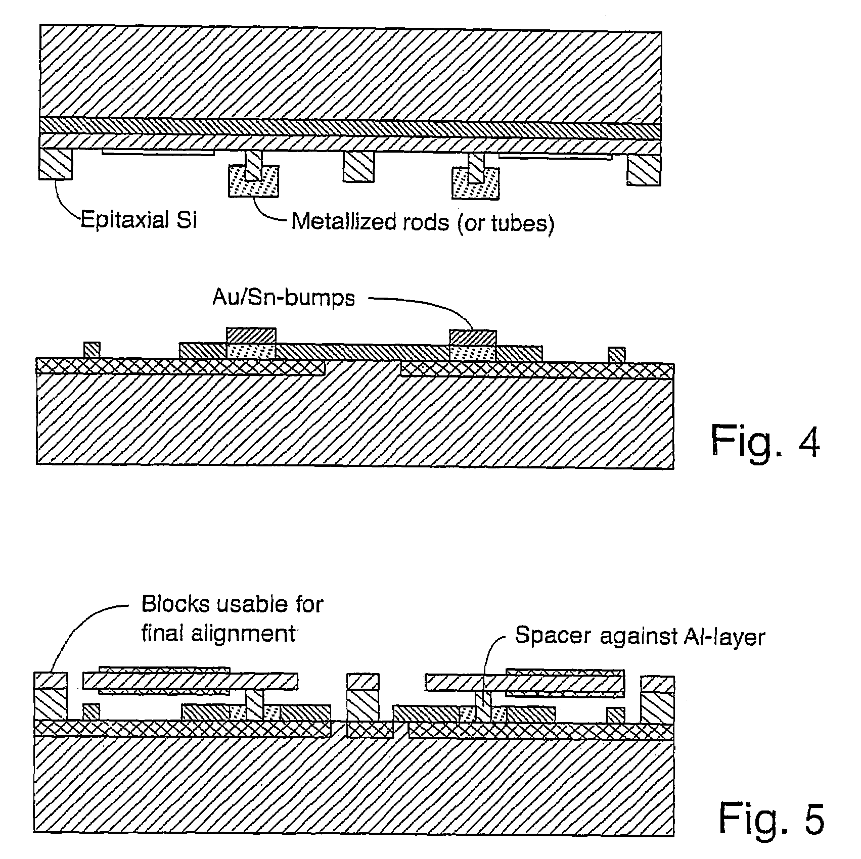
[0085]FIG. 9 schematically shows a perspective view of a fourth embodiment of the final mirror or mirror arrays device fabricated according to the invention. For clarity the mirrors and hinge / suspension structures are removed in the right part of the drawing looking into the cavity where the electrodes are shown. FIG. 10 is a cross section at A–A′ in FIG. 9.

[0086]The process comprises making two separate wafers, a first wafer carrying the mono / single crystalline materials, e.g. silicon, GaAs, SiC etc, from which the mirror(s) are to be made, and a second wafer carrying components necessary for the function of the final mirror device such as electrodes, bond pads, via contacts, CMOS electronics. Then the two wafers are bonded together using an eutectic bonding method according to the present invention.

[0087]In summary the process can be described as follows:

[0088]Making the SOI-wafer (Top-wafer, FIG. 11):[0089]1.—Evaporation or sputtering of thin layers of Ti / Au as electrode structur...

embodiment 5

[0116]Similiar structure as embodiment 4 but placing the solder on top wafer and contact areas on the bottom wafer (as embodiment 1 but with the final structure according to embodiment 4).


PUM

PropertyMeasurementUnit
pressureaaaaaaaaaa
temperaturesaaaaaaaaaa

Abstract

A method of making a deflectable, free hanging micro structure having at least one hinge member, the method includes the steps of providing a first sacrificial wafer having a single crystalline material constituting material forming the micro structure. A second semiconductor wafer including necessary components for forming the structure in cooperation with the first wafer is provided. Finite areas of a structured bonding material is provided, on one or both of the wafers at selected locations, the finite areas defining points of connection for joining the wafers. The wafers are bonded using heat and optionally pressure. Sacrificial material is etched away from the sacrificial wafer, patterning the top wafer by lithography is performed to define the desired deflectable microstructures having hinges, and subsequently silicon etch to make the structures.

Description

[0001]This application is a 371 of national stage application of PCT / SE03 / 00252, Feb. 14, 2003, which claims benefit under 35 USC 119(e) of 60 / 356,165, Feb. 14, 2002.TECHNICAL FIELD[0002]The present invention relates generally to processes for the manufacture of free-hanging micro structures, in particular such structures as mirrors for use in Spatial Light Modulation (SLM) devices, by employing mirror arrays.[0003]In particular it relates to novel processes for the manufacture of mirror structures suitable i.a. for SLM.BACKGROUND OF THE INVENTION[0004]Spatial light modulators (SLM) are transducers that modulate incident light in a spatial pattern corresponding to an electrical or optical input. The incident light may be modulated in its phase, intensity, polarization, or direction, and the light modulation may achieved by a variety of materials exhibiting various electrooptic or magnetoopotic effects and by materials that modulate light by surface deformation. SLMs have found numer...

Claims


Application Information

Patent Timeline
Patent Type & Authority Patents(United States)
IPC IPC(8): H01L21/00B81B3/00B81B7/04G02F1/29H01L21/30H01L21/302H01L21/46H01L21/461
CPCB81C1/00142B81C1/0015B81C3/002B81B2201/042B81C2203/058B81C2201/019B81C2201/0191
Inventor KAELVESTEN EDVARDEBEFORS THORBJOERNSVEDIN NIKLASWESTIN H DOT OVER AKAN
Owner SILEX MICROSYST
Why Eureka
Try Eureka