Process for fabricating non-volatile memory by tilt-angle ion implantation

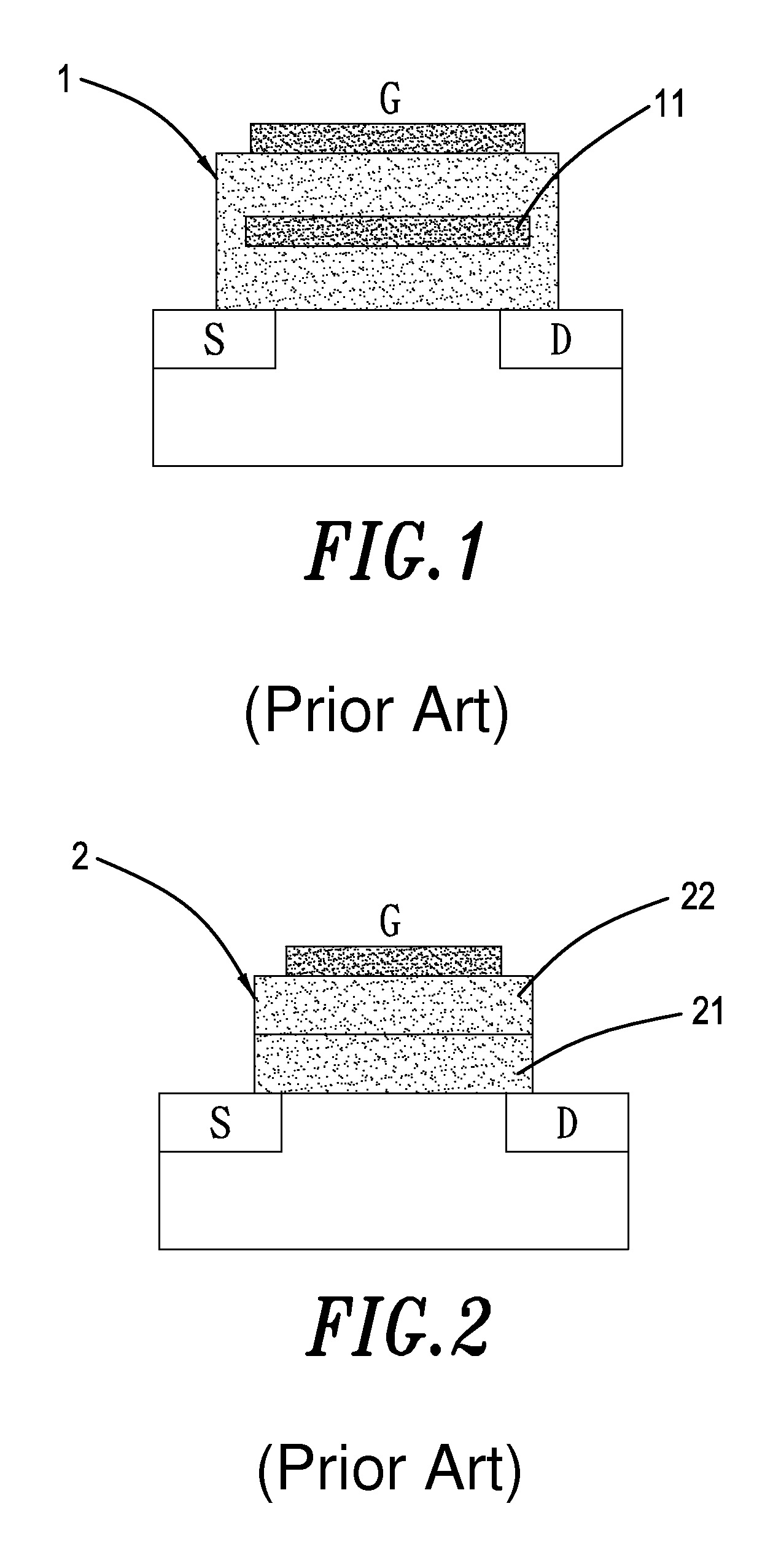
a technology of non-volatile memory and ion implantation, which is applied in the direction of basic electric elements, electrical apparatus, semiconductor devices, etc., can solve the problems of loss of electrons stored, substantial economic benefit, and increase in production costs, and achieve the effect of lowering production costs

Inactive Publication Date: 2007-02-20
CHUNG YUAN CHRISTIAN UNIVERSITY
View PDF3 Cites 4 Cited by
  • Summary
  • Abstract
  • Description
  • Claims
  • Application Information

AI Technical Summary

Benefits of technology

[0010]One object of the invention is to provide a process for fabricating non-volatile memory by tilt-angle ion implantation characterized in that two bits can be stored in a single cell to achieve the result of lowering production cost.
[0011]Another object of the invention is to provide a process for fabricating non-volatile memory by tilt-angle ion implantation characterized in that ions of heterogeneous elements are implanted sideling within the nitride dielectric materials in a manner that the nitride dielectric material forms traps to capture electrons more easily that renders merge together of electrons not increased easily along with the operation time so as to achieve effects of good programming and erasing.
[0012]Still another object of the invention is to provide a process for fabricating non-volatile memory by tilt-angle ion implantation characterized in that both ends of the upper and lower oxide layers are etched off by the step of etching to reduce the structural destruction of oxide layers due to implantation of heterogeneous elements to achieve the purpose of the promotion of the reliability of devices.
[0013]The process for fabricating non-volatile memory by tilt-angle ion implantation according to the invention that can achieve the above-described objects comprises essentially of implanting sideling within the nitride layer that can capture electrons of heterogeneous elements such as Ge, Si, N2, O2, and the like, for the purpose of giving the nitride an electron trap density deeper than the original one such that electrons can be retained steadily within the nitride without loss; etching off the oxide layer that is damaged due to the implantation, depositing an interstitial wall for the oxide layer to solve effectively the effect on the device caused by the implantation of the heterogeneous element and thereby to improve issues of retention time of bit merge occurred to the current silicon-oxygen-nitrogen-oxygen-silicon compound (SONOS).

Problems solved by technology

However, the floating gate device 1 can store only one bit so that its production cost is correspondingly increased and hence exhibit substantially no economical benefit.
Unfortunately, the charge trapping device 2 shows a big problem on retention time, because oxides 21 in the underlying layer might capture positive charge therein during programming that may lower the energy barrier of the underlying oxide layer 21 and as a result, electrons captured in the silicon nitride 22 might penetrate readily through the underlying oxide layer 21.
This would cause loss of electrons stored therein and consequently reduces the retention time.
This mechanism is the biggest problem encountered in the current 2-bit storage.
Accordingly, it is apparent that the conventional device has many disadvantages and is not a perfect design such that it is desirable to be improved.

Method used


Image

  • Process for fabricating non-volatile memory by tilt-angle ion implantation
  • Process for fabricating non-volatile memory by tilt-angle ion implantation
  • Process for fabricating non-volatile memory by tilt-angle ion implantation

Examples


Embodiment Construction

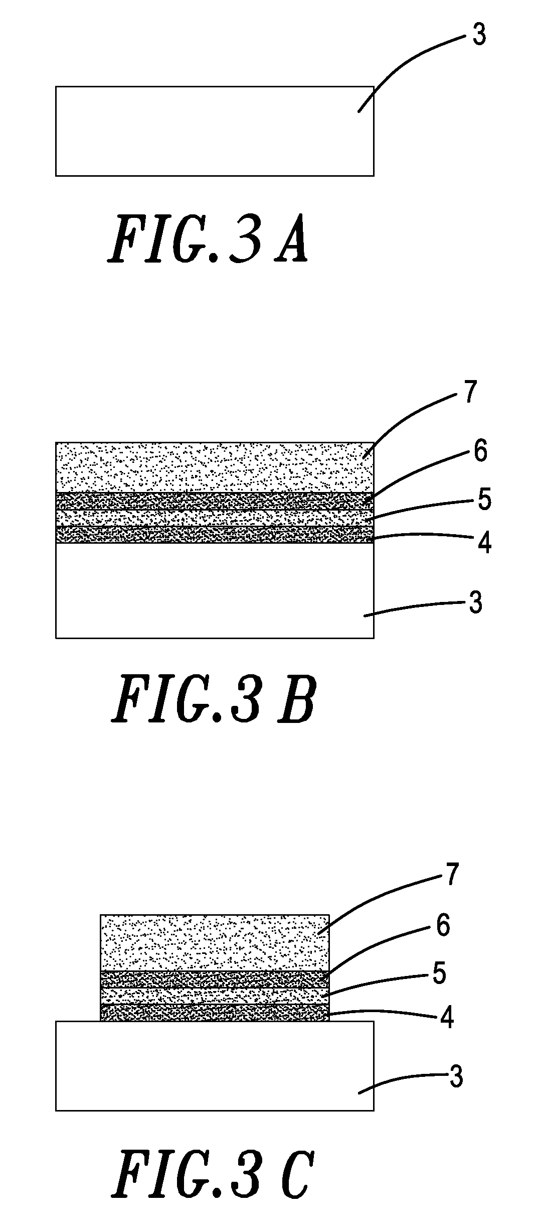
[0018]Referring to FIGS. 3A–3F, a process for fabricating non-volatile memory by tilt-angle ion implantation according to the invention comprises the steps of:

[0019]step 1: providing a wafer substrate 3 (FIG. 3A);

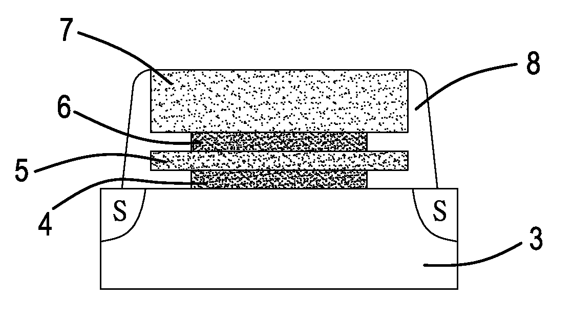
[0020]step 2: depositing over the wafer substrate 3 successively a first oxide layer 4, nitride layer 5, an upper second oxide layer 6, and a gate 7, in a manner that a gate dielectric layer (oxide-nitride-oxide (ONO)) is formed over the wafer substrate 3 (FIG. 3B), wherein said nitride layer 5 can store two bits at the same time; said first and second oxide layers 4, 6 may be silicon oxide; said gate layer 7 is a polysilicon layer; and said nitride layer 5 is silicon nitride;

[0021]step 3: forming gate pattern by photoresist developing, and removing both ends of the gate dielectric layer by directional etching to expose said first oxide layer or said substrate (FIG. 3C);

[0022]Step 4: removing the photoresist and using tilt-angle ion implantation to implant within said nitri...


PUM

PropertyMeasurementUnit
incident angleaaaaaaaaaa
tilt angleaaaaaaaaaa

Abstract

A process for fabricating non-volatile memory by tilt-angle ion implantation comprises essentially the steps of implanting sideling within a nitride dielectric layer heterogeneous elements such as, for example, Ge, Si, N2, O2, and the like, for forming traps capable of capturing more electrons within the nitride dielectric layer such that electrons can be prevented from binding together as the operation time increased; etching off both ends of the original upper and underlying oxide layers to reduce the structural destruction caused by the implantation of heterogeneous elements; and finally, depositing an oxide gate interstitial wall to eradicate electron loss and hence promote the reliability of the device.

Description

BACKGROUND OF THE INVENTION[0001]1. Field of the Invention[0002]The invention relates to a process for fabricating non-volatile memory by tilt-angle ion implantation, and in particular, to a process for fabricating non-volatile memory by tilt-angle ion implantation characterized in that, in addition to increase the retention time of the memory, it can avoid merge of electrons due to prolonged operation.[0003]2. Description of the Prior Art[0004]Recently, the role of the flash memory device in the development and fabrication of the semiconductor device has becomes more and more important. As portable electronic products increasingly prevail, the modification and portability of data has a pivotal function in these products, and accordingly, a flash memory has its competitive advantage over other devices.[0005]Referring to FIGS. 1 and 2, a schematic structure of a conventional non-volatile memory is shown to be composed of two different structures: a floating gate device 1 (FIG. 1) and...

Claims


Application Information

Patent Timeline
Patent Type & Authority Patents(United States)
IPC IPC(8): H01L21/336
CPCH01L21/28282H01L29/7923H01L29/4234H01L29/40117
Inventor JENG, ERIK S.CHOU, WU-CHINGWU, LI-KANGLI, CHIEN-CHEN
Owner CHUNG YUAN CHRISTIAN UNIVERSITY
Why Eureka
Try Eureka