Method for electron beam-initiated coating for application of transmission electron microscopy

a transmission electron microscopy and electron beam technology, applied in material analysis using wave/particle radiation, instruments, nuclear engineering, etc., can solve the problems of amorphous damage ranging in thickness from 1, 10 nanometers, and adversely affecting the quality of tem analysis

Inactive Publication Date: 2007-02-20
IBM CORP
View PDF9 Cites 18 Cited by
  • Summary
  • Abstract
  • Description
  • Claims
  • Application Information

AI Technical Summary

Problems solved by technology

In both cases, amorphous damage ranging in thickness from 1–10 nanometers may result, particularly in the case of ion milling.
This amorphous damage adversely affects the quality of the TEM analysis because it alters the natural characteristics of the material.
Moreover, a typically applied process of ion beam initiated metal encapsulation can cause edge roundness, flat top edge rounding and blurred boundary definition, which raises a serious issue if TEM is used to place emphasis on the feature topography, such as true feature boundary definition for critical dimension (CD) measurement.

Method used


Image

  • Method for electron beam-initiated coating for application of transmission electron microscopy
  • Method for electron beam-initiated coating for application of transmission electron microscopy
  • Method for electron beam-initiated coating for application of transmission electron microscopy

Examples


Embodiment Construction

[0016]Disclosed herein is a method for transmission electron microscopy (TEM) sample preparation in which only the area of interest is covered with a conductive metal layer such as platinum. Briefly stated, an initial thickness of conductive metal (e.g., platinum) is locally formed by electron beam (i.e., low-energy) deposition, which protects the topographic features on the surface of the tested sample. Thereafter, this precoated layer may optionally be coated with additional metal formed by ion beam (i.e., high-energy) deposition for increased throughput. In so doing, the damage created on the surface of interest can be minimized.

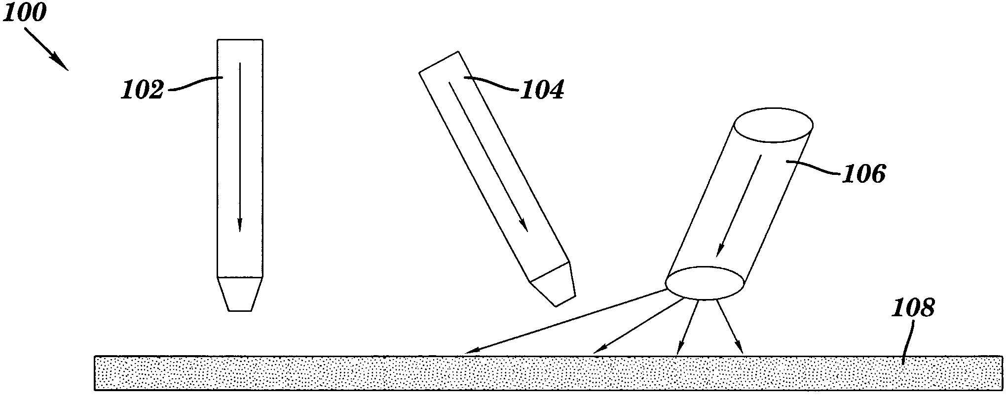
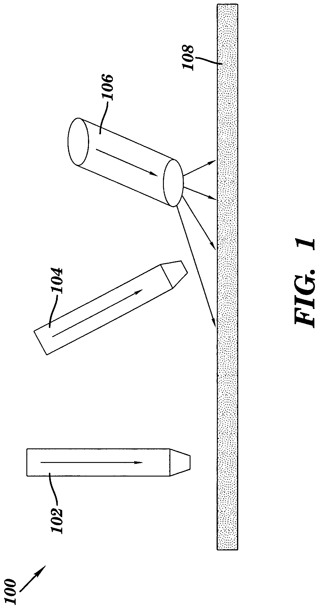
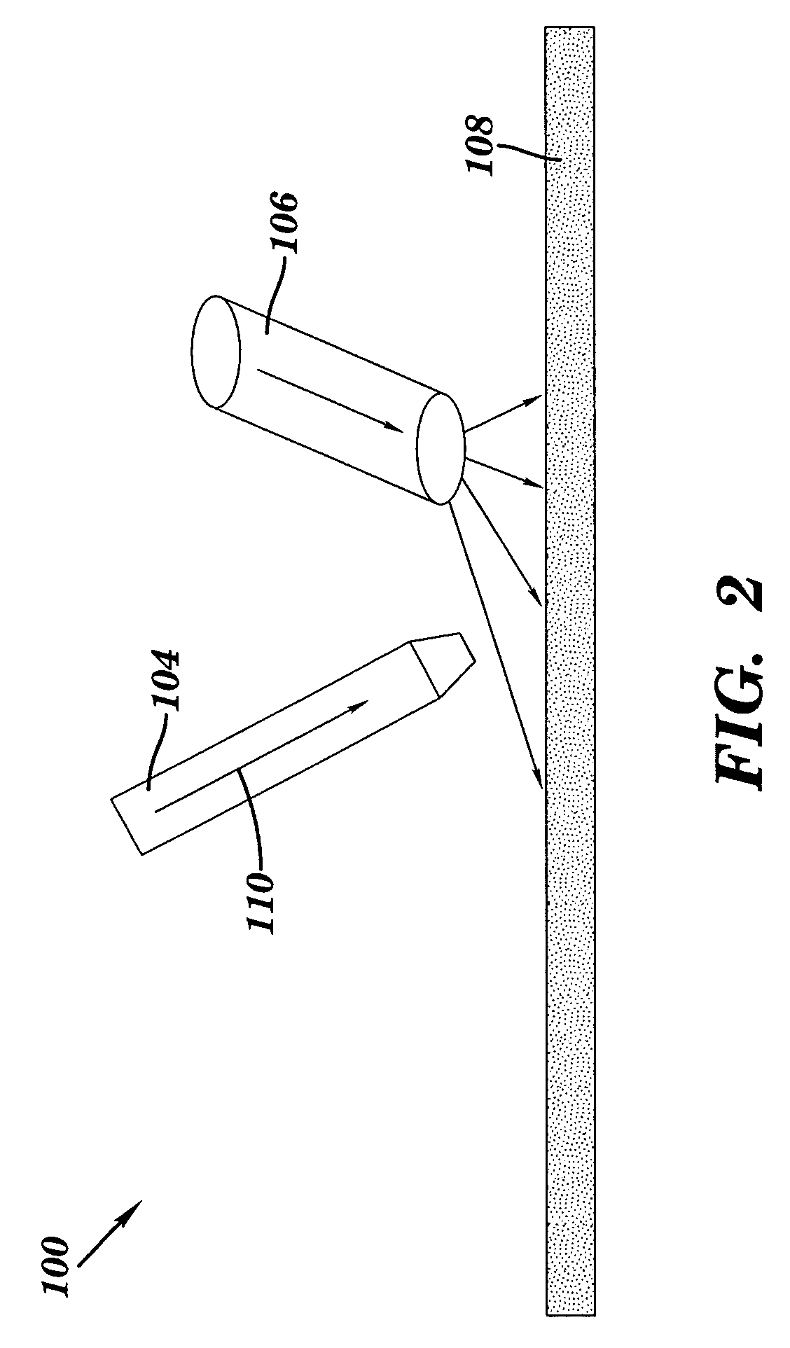
[0017]Referring initially to FIG. 1, there is shown a side sectional view of a tunneling electron microscopy (TEM) preparation system 100 suitable for use in accordance with an embodiment of the invention. System 100 includes a focused ion beam (FIB) column 102, a scanning electron microscope (SEM) column 104 and a precursor delivering tube 106 for supply...


PUM

PropertyMeasurementUnit
thicknessaaaaaaaaaa
thicknessaaaaaaaaaa
thicknessaaaaaaaaaa

Abstract

A method for preparing a specimen for application of microanalysis thereto includes forming an initial conductive layer over a defined area of interest on a semiconductor substrate, the initial conductive layer formed through an electron beam deposition process. A volume of substrate material surrounding the area of interest is removed, thereby forming the specimen, including said area of interest and said initial conductive layer over the area of interest. The specimen is then removed from the bulk substrate material.

Description

BACKGROUND OF INVENTION[0001]The present invention relates generally to inspection of integrated circuit devices, and, more particularly, to a method for preparing a specimen for application of microanalysis, such as transmission electron microscopy (TEM).[0002]Advancements in Transmission Electron Microscopy, or TEM, technology enables materials to be analyzed at near atomic resolution by providing high-magnification, high-resolution imaging and analysis capabilities. TEM enables scientists to gather information relating to a material's physical properties, such as its microstructure, crystalline orientation and elemental composition. This information has become increasingly important as the need for advanced materials for use in areas such as microelectronics and optoelectronics, biomedical technology, aerospace, transportation systems and alternative energy sources, among others, increases.[0003]TEM is accomplished by examining material specimens under a transmission electron mic...

Claims


Application Information

Patent Timeline
Patent Type & Authority Patents(United States)
IPC IPC(8): G01N31/00G01N23/00G01N33/00G21K7/00
CPCG01N1/32
Inventor LU, WEI
Owner IBM CORP
Why Eureka
Try Eureka