
Apparatus for wafer inspection

Active Publication Date: 2007-02-20
LEICA MICROSYSTEMS SEMICON GMBH
View PDF11 Cites 13 Cited by
  • Summary
  • Abstract
  • Description
  • Claims
  • Application Information

AI Technical Summary

Benefits of technology

[0010]It is therefore the object of the present invention to describe an apparatus with which regions from which resist has been removed, in particular edge-bead-removed regions, can reliably be made visible and the quality of the edge bead removal can easily be determined or assessed.
[0017]Although edge regions of the wafer are preferably inspected, according to the present invention any other desired regions on the surface of a wafer or semiconductor substrate can also, in principle, also be inspected, for which purpose the illuminating light is directed appropriately onto the region to be inspected, and the light reflected there is imaged appropriately into the imaging device. For imaging of the illuminating light and of the light reflected from the surface, further imaging means, for example deflecting mirrors, prisms, or the like, can be introduced into the beam path so that the apparatus can be configured in even more variable fashion.
[0020]The transmission axes of the two polarizing means are preferably aligned relative to one another so that an optimum contrast between treated and untreated surface regions of the wafer can be achieved. For this purpose, the transmission axes are preferably coordinated with one another, using light that is reflected exclusively from untreated or treated surface regions of the wafer, in such a way that the light behind the polarizing means associated with the imaging device substantially disappears (zero balancing). This has the advantage that the gain of the imaging device can be set relatively high, so that even very small intensity changes, brought about by changes in the polarization state of the light reflected at surface regions having differing properties, will result in relatively large signal amplitudes. The aforesaid zero balancing is preferably performed on the basis of the surface regions that predominate in terms of area. For example, if a comparatively small edge-bead-removed region is to be determined and assessed, the aforesaid zero balancing operation is preferably performed on the basis of regions from which no resist has been removed.
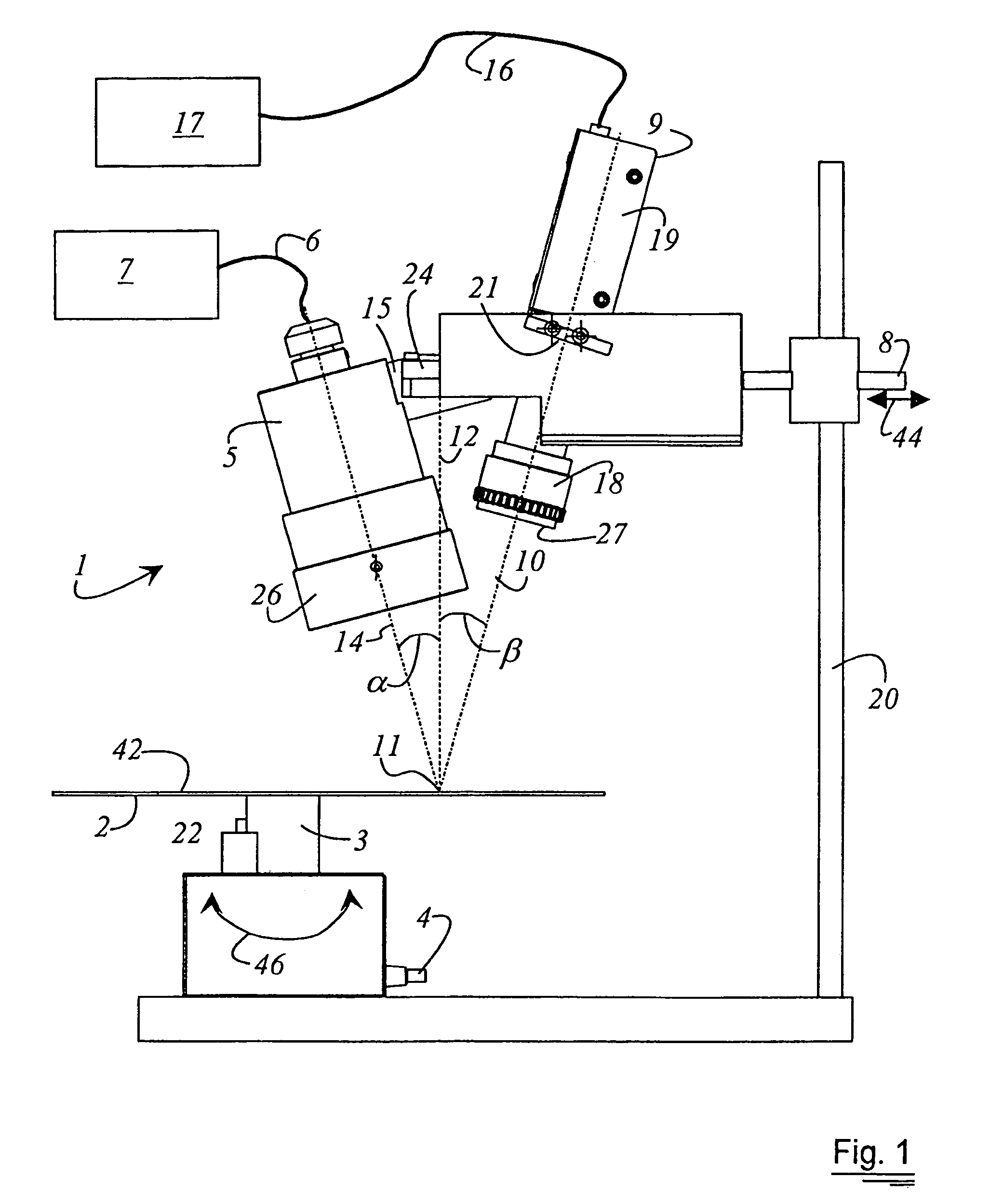
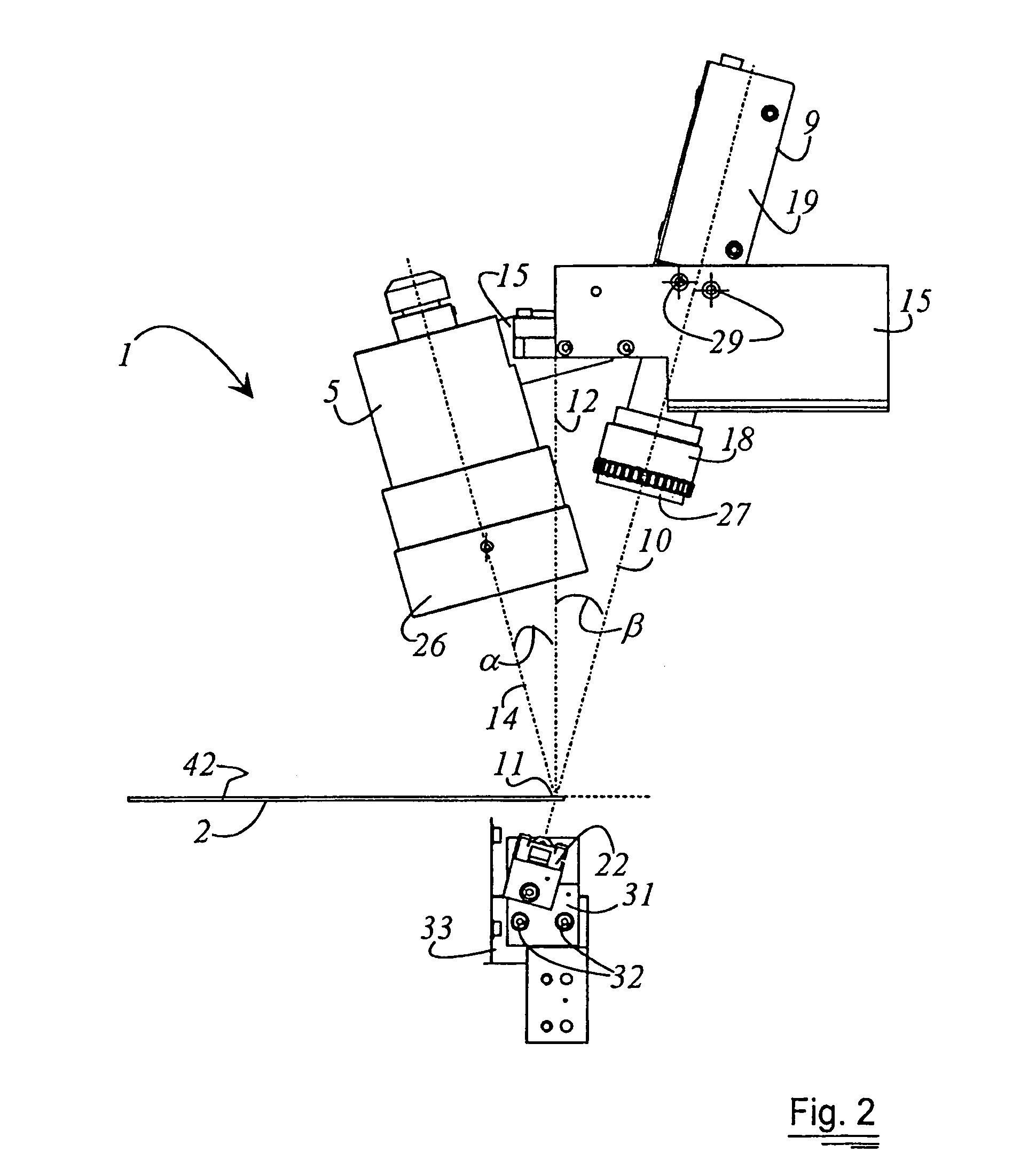
[0023]According to a first preferred embodiment, the illumination angle α corresponds to the Brewster angle of the material of the wafer to be inspected, for example silicon, or of a layer applied onto the wafer to be inspected, for example a photoresist layer that is to be removed from the edge region. In this case the light reflected from the material or from the layer applied thereonto is reflected in such a way that it is polarized perpendicular to the image plane extending between the illumination axis and image axis. The aforementioned zero balancing can thus easily be performed by simply rotating the polarizing means associated with the imaging device, so that its transmission axis lies in the image plane. Although the term “zero balancing” is used hereinafter, it should be noted that this can also be incomplete, as a result in particular of inhomogeneities and irregularities on the surface of the wafer to be inspected. In order to perform the aforementioned zero balancing, it may also be advantageous if the illumination angle α does not correspond exactly to the Brewster angle, but instead is inclined at a preferably small angle toward or away from the wafer normal line. This makes it possible, for example, to compensate for inhomogeneities and irregularities on the surface of the wafer to be inspected.
[0024]According to a further preferred embodiment, the illumination angle α is relatively small, so that the illuminating light is incident at a relatively steep angle onto the surface to be inspected. The illumination angle α is preferably in the range from approximately 7 degrees to approximately 20 degrees, preferably in the range from approximately 14 degrees to approximately 16 degrees in order to produce even more advantageous properties for zero balancing, and in even more preferred fashion it is approximately 15 degrees in order to achieve even more advantageous zero balancing properties. This takes into account the effect that thin, relatively regular features, for example conductor paths, circuit features, etc, that are often provided on the wafer surface act like a groove grating, thus resulting in diffraction effects and polarization effects. These can have an influence on the aforementioned zero balancing, which can be compensated for by setting the illumination angle to a relatively steep incidence angle. In principle, a stepless transition between the aforementioned Brewster angle and the relatively steep incidence angle just mentioned is possible for illumination angle α.
[0025]The illumination device can be equipped both with a polychromatic and with a monochromatic light source. For example, the light source can be a mercury vapor lamp or a cold light source having an attached fiber bundle for transmitting the light. The use of an LED or a laser with beam spreading is also conceivable. Both a divergent and a convergent illumination beam path are usable. In a preferred embodiment, a telecentric illumination beam path is preferred, slight deviations from strictly telecentric beam guidance being permissible with no loss of illumination quality.

Problems solved by technology

The photoresist at the edge of the wafer, and the edge bead, can lead to contamination of production machinery and to the creation of defects on the wafer in subsequent process steps.
Errors in the width of the edge bead removal derive from inaccurate alignment of the corresponding edge bead removal devices relative to the wafer.
Inaccurate alignment of the illumination devices relative to the wafer upon exposure of the photoresist constitutes a further error source.
Edge bead removal over too wide an edge region results in a decrease in the usable wafer area, and thus in a loss of chip production.
Insufficient edge bead removal can result, in the edge region of the wafer, in contamination of the subsequently applied resist layers or other features.
Incomplete bead removal in the edge region can also, upon handling of the wafer by means of handling tools which, for example, engage into the edge region of the wafer, lead to impurities, e.g. abraded material, which cause contamination of the rest of the wafer surface and diminished quality in downstream process steps.
In the known apparatuses for wafer inspection, the quality of the edge bead removal cannot easily be determined and assessed.
It is moreover difficult to make a distinction between the edge bead removal (EBR) and the other edges present in the image.
It is therefore very difficult or impossible to filter out the edge bead removal in this fashion using an image processing system.
Even a visual inspection by an observer produces no better results, since the human eye also cannot manage to allocate the various edges and observed colors or grayscale values to the various process steps.

Method used


Image

  • Apparatus for wafer inspection
  • Apparatus for wafer inspection
  • Apparatus for wafer inspection

Examples


Embodiment Construction

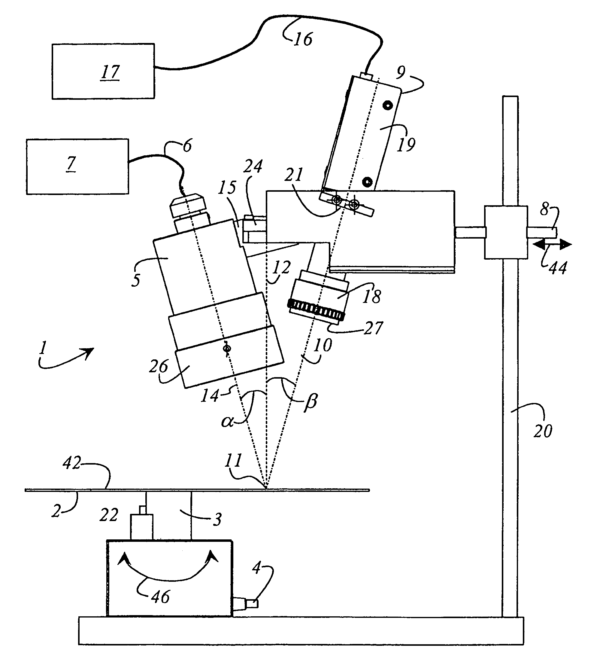
[0039]FIG. 1 shows an apparatus 1 for wafer inspection with a wafer 2 to be inspected. Wafer 2 is placed onto a receiving device 3 that retains wafer 2 by vacuum suction. The necessary vacuum is conveyed to receiving device 3 by means of a vacuum line 4 that is connected to a vacuum system (not depicted) for generating the vacuum.

[0040]An incident-light illumination device 5, to which light is conveyed from a light source 7 via a light-guide bundle 6, is directed onto a region to be inspected of wafer 2. Incident-light illumination device 5 is arranged at an inclination with respect to surface 42 of wafer 2. An imaging device 9 is arranged on a longitudinally displaceable support element 8. The direction of the longitudinal displacement is indicated by double arrow 44. Imaging device 9 has an image axis 10. Defined at incidence point 11 of this image axis 10 on wafer 2 is a wafer normal line 12, i.e. a construction line that is perpendicular to wafer 2 at incidence point 11. In the ...


PUM


Abstract

An apparatus for wafer inspection is described, comprising an incident-light illumination device (5) having an illumination axis and an imaging device (9) having an image axis, both of which are inclined with respect to one another and are directed onto a region to be inspected of the surface (42) of a wafer (2). According to the present invention, the apparatus is characterized in that the incident-light illumination device (5) and the imaging device (9, 19) each have associated with them a polarizing means whose transmission axes are oriented at a predetermined angle to one another.

Description

CROSS REFERENCE TO RELATED APPLICATIONS[0001]This application claims priority of the German patent application 103 24 474.3 which is incorporated by reference herein.FIELD OF THE INVENTION[0002]The invention concerns an apparatus for wafer inspection.BACKGROUND OF THE INVENTION[0003]In semiconductor production, wafers are coated with photoresist during the production process. The photoresist passes first through an exposure process and then a development process. In these processes, it is patterned for subsequent process steps. For production-related reasons, slightly more photoresist becomes deposited in the edge region of the wafer than in the middle of the wafer. An “edge bead” is thereby formed. The photoresist at the edge of the wafer, and the edge bead, can lead to contamination of production machinery and to the creation of defects on the wafer in subsequent process steps.[0004]To eliminate these effects, an edge bead removal (EBR) process is performed. Errors in the width of...

Claims


Application Information

Patent Timeline
IPC IPC(8): G01N21/00G01N21/88G01N21/95
CPCG01N21/8806G01N21/9503G01N21/9501
Inventor KREH, ALBERTBACKHAUSS, HENNING
Owner LEICA MICROSYSTEMS SEMICON GMBH
Learn More