Eureka AIR delivers breakthrough ideas for toughest innovation challenges, trusted by R&D personnel around the world.

Semiconductor integrated circuit and electronic system

a technology of integrated circuits and semiconductors, applied in the direction of instruments, pulse automatic control, transistors, etc., can solve the problems of increasing the size of the module, disturbing the miniaturization of the system, and difficulty in realizing, so as to reduce the chip size and the module size

Inactive Publication Date: 2007-02-27
RENESAS TECH CORP
View PDF3 Cites 26 Cited by
  • Summary
  • Abstract
  • Description
  • Claims
  • Application Information

AI Technical Summary

Benefits of technology

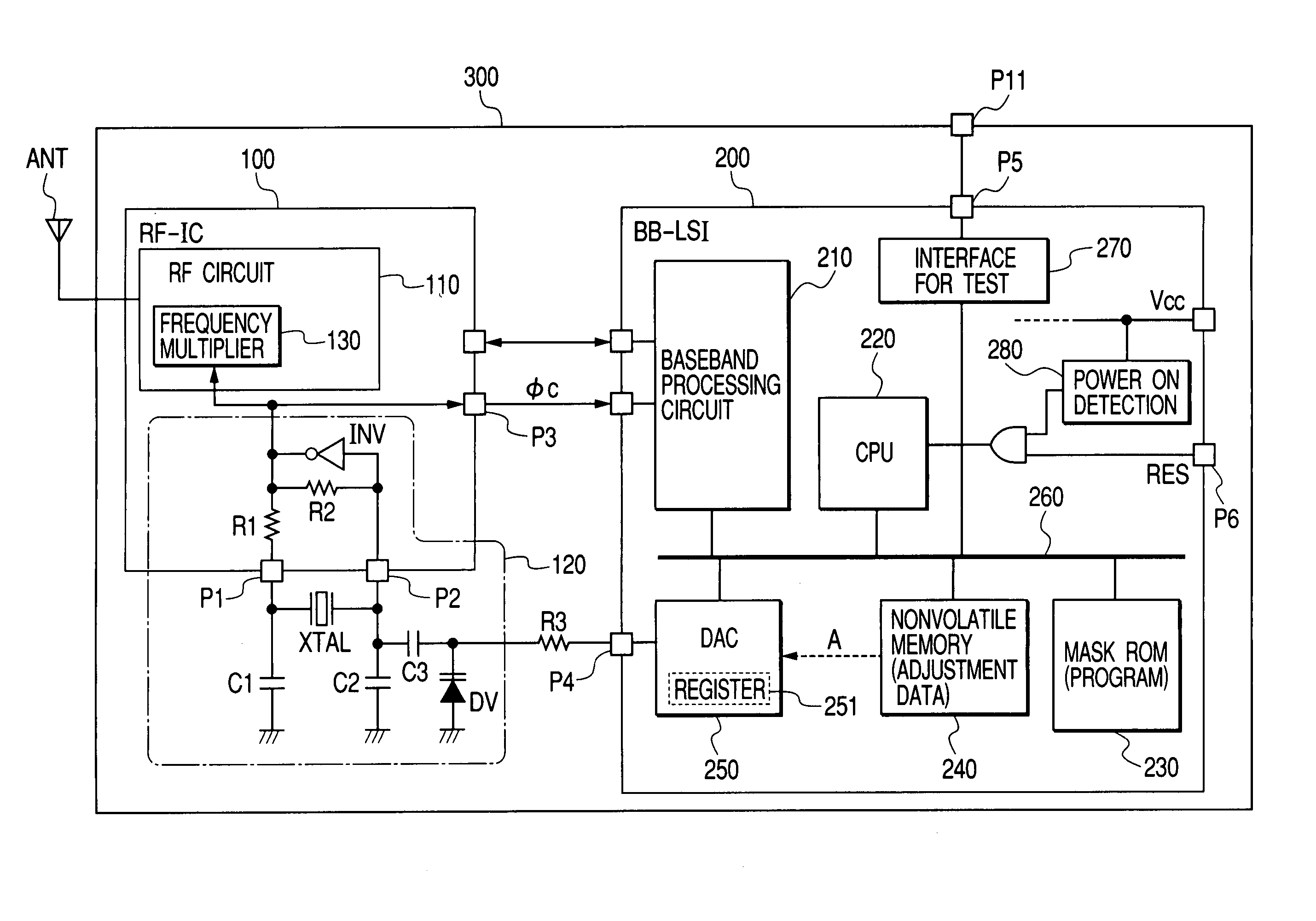
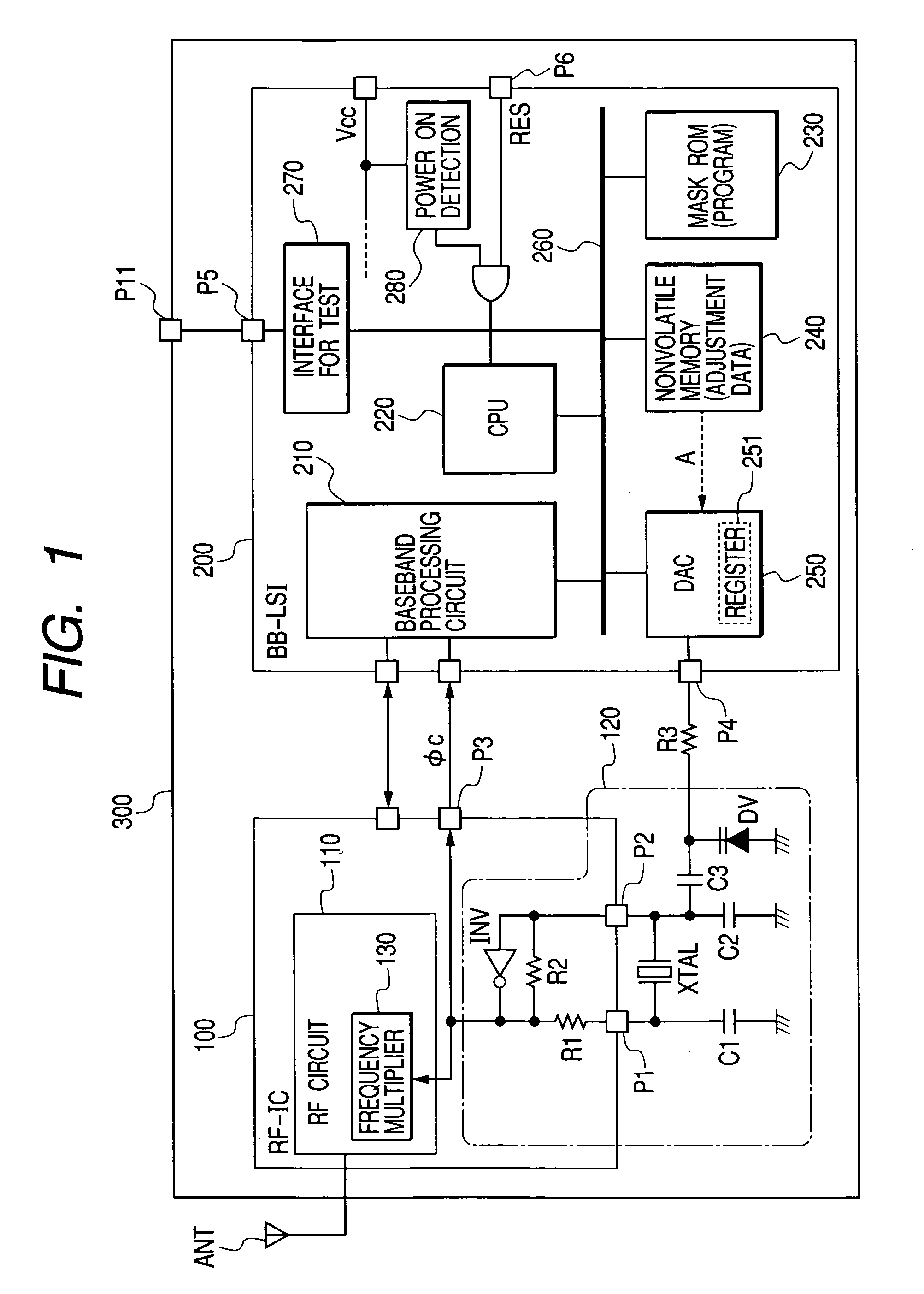
[0014]An object of the invention is to provide a semiconductor integrated circuit for communication control and a wireless communication system using the same, which realize smaller sizes of a chip and a module by enabling trimming data to be written into a nonvolatile memory without increasing the number of external terminals.
[0015]Another object of the invention is to provide a semiconductor integrated circuit for communication control and a wireless communication system using the same which realize higher mass productivity and lower manufacturing cost by shortening time required to write a nonvolatile memory. Further, the invention provides a technique which can be applied not only to the semiconductor integrated circuit for communication control and the wireless communication system but also to other semiconductor integrated circuits and electronic systems.
[0020]By the means, without increasing the number of external terminals and external circuits, trimming data can be written to the nonvolatile memory, so that the size of the chip and the size of the module can be reduced and, also in the case where the characteristics of the circuit change during use, the trimming data can be rewritten. According to the invention, changes in the circuit characteristics caused due to not only variations in electronic parts but also variations in elements constructing the circuit can be corrected.
[0022]By the means, a process of writing a program into a nonvolatile memory becomes unnecessary. Thus, time required for writing the nonvolatile memory is shortened, mass productivity can be increased, and the manufacturing cost can be reduced. In a system on which a mask ROM for storing a program, formed as a separate chip and a semiconductor integrated circuit having therein the nonvolatile memory are mounted, as an input pin and an interface circuit used for sending and storing the trimming data to the nonvolatile memory, a pin such as a test pin and an interface circuit which are originally provided for the board are used. With the configuration, the size of the module can be reduced.
[0024]By the means, without increasing the number of external terminals, trimming data and data peculiar to the system stored in the nonvolatile memory can be rewritten. Consequently, the size of the chip and the size of the module can be reduced. Necessary data can be written in a state where the semiconductor integrated circuit is mounted on the module board and, also in the case where the system configuration of operation mode is changed, the data can be rewritten.

Problems solved by technology

It was found to be difficult to realize it since there are physical limitations on an external circuit and the number of terminals which can be provided for the module.
When such an external circuit and terminals are provided for the module, the size of the module increases and it disturbs miniaturization of the system.

Method used


Image

  • Semiconductor integrated circuit and electronic system
  • Semiconductor integrated circuit and electronic system
  • Semiconductor integrated circuit and electronic system

Examples


second embodiment

[0074]the invention will now be described with reference to FIG. 5.

[0075]In the second embodiment, some upper bits (for example, five bits) in the frequency trimming data of the quartz oscillating circuit 120 are stored in the nonvolatile memory 240, and some lower bits (for example, three bits) are supplied from the register 252 which can be set by the CPU 220. With the configuration, the invention can be also adapted to a system in which oscillation frequency changes depending on the environment.

[0076]Generally, in the Bluetooth system, as shown in FIG. 4, the master device 610 and the slave devices 620 to 640 have the Bluetooth clocks and perform communications synchronously with each other. The clock of any of the devices has precision of 3.2 kHz +−20 ppm according to standard. The clocks, however, cannot be perfectly made coincide with each other and a deviation occurs with time. In the conventional Bluetooth system, even when clocks are deviated from each other, the frequency ...

first embodiment

[0086]The embodiment does not deny the function of adjusting the frequency of the quartz oscillating circuit 120 on the RF IC 100 side with the trimming data stored in the nonvolatile memory 240 like in the Both the frequency trimming data and the communication parameters can be stored in the nonvolatile memory 240.

[0087]FIGS. 7 and 8 show that, in place of a terminal for setting the mode of the LSI, mode setting data stored in the nonvolatile memory 240 is used. A Bluetooth communication system will be described as an example. A plurality of RF ICs of some manufacturers of different system of transmitting / receiving signals to / from the baseband LSI are provided. It is convenient for an assembly maker that an arbitrary RF IC can be selected and combined with the baseband LSI.

[0088]In the baseband LSI 200 shown in FIG. 7, interfaces which can be connected to a plurality of RF ICs having different functions and specifications of terminals are provided in an interface portion with the ...


PUM


Abstract

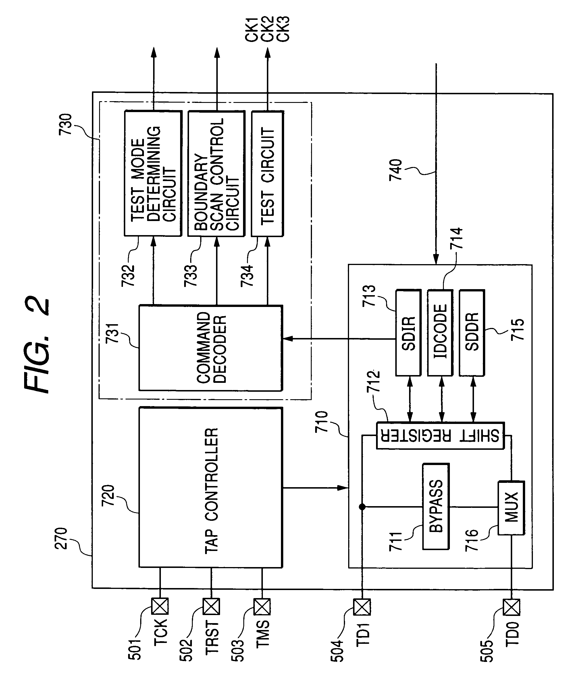
The invention provides a semiconductor integrated circuit for communication control and a wireless communication system using the same realizing reduction in the size of a chip and the size of a module by enabling trimming data to be written into a nonvolatile memory without increasing the number of external terminals. A rewritable nonvolatile memory is provided in a semiconductor integrated circuit, characteristics of circuits including an electronic part are measured and trimming data for correcting variations in the characteristics is stored in the nonvolatile memory. A pin and an interface circuit such as a test pin and a JTAG interface circuit which are originally provided for the semiconductor integrated circuit also serve as an input pin and an interface circuit for sending and storing the trimming data to the nonvolatile memory.

Description

CROSS-REFERENCE TO RELATED APPLICATION[0001]The present application claims priority from Japanese patent application JP 2003-182258 filed on Jun. 28, 2003, the content of which is hereby incorporated by reference into this application.BACKGROUND OF THE INVENTION[0002]The present invention relates to a technique effective when applied to adjustment of a change in a circuit characteristic due to variations in external electronic parts or devices of a semiconductor integrated circuit (hereinbelow, also written as IC), particularly, adjustment of a frequency shift of an oscillator having an oscillating element. More particularly, the invention relates to a technique effective when applied to an IC for communication control of, for example, a Bluetooth communication standard and a communication system using the IC.[0003]One of wireless communication standards is the standard called Bluetooth for a short-distance wireless communication using a frequency band from 2.4 GHz to 2.48 GHz. A wi...

Claims


Application Information

Patent Timeline
IPC IPC(8): G11C29/00H03L7/00H03L7/06H01L21/822G11C7/10G11C16/04G11C29/02H01L21/82H01L21/8247H01L27/04H01L27/10H01L27/115H01L29/788H01L29/792H03B5/32
CPCG11C7/1006G11C16/0433G11C16/0441G11C29/028G11C29/12015G11C29/50012G11C29/02G11C2216/10
Inventor KOJIMA, HIROTSUGUKITAMURA, TERUO
Owner RENESAS TECH CORP
Why Eureka
Eureka Blog
Learn More