Charge multiplier with logarithmic dynamic range compression implemented in charge domain

a charge domain and multiplier technology, applied in the field of solid state image sensors, can solve the problems of reducing the noise floor of the present day charge conversion amplifier, affecting the ionization, and the design of the ccd register, and achieves high dr, high charge to voltage conversion gain, and high performance

Active Publication Date: 2007-03-13
ISETEX
View PDF2 Cites 24 Cited by
  • Summary
  • Abstract
  • Description
  • Claims
  • Application Information

AI Technical Summary

Benefits of technology

[0012]It is yet another object of the invention to provide a practical high performance image sensors of various architectures that have high DR. These and other objects are achieved by incorporating Charge Multiplier cells into a horizontal register of a CCD image sensor and combine them with the DR compression mechanism. As charge is multiplied the horizontal register would normally have to be increased in width to accommodate more charge and have larger or more charge multiplication gates per stage. This is avoided if the charge overflow region is incorporated into the same cells with the charge multiplier.
[0013]As charge is multiplied to a predetermined threshold level the amount of charge exceeding that threshold is split off into an adjacent overflow CCD register. The adjacent register, which does not include the charge multiplication gate

Problems solved by technology

The suitable clocking voltages generate high fields in the structure, and when a carrier is injected into these high field regions, it gains energy and may cause impact ionization.
The noise floor of the present day charge conversion amplifiers is approximately 10 electrons, and cannot be easily reduced.
The charge multiplication, however, presents a problem for the design of the CCD registers.
This may not be easily accomplished in the registers that are restricted in both dimensions by the sensor pixel size.
A second problem resulting from the charge multiplication is related to the DR of the charge conversion structures at the input of the charge det

Method used


Image

  • Charge multiplier with logarithmic dynamic range compression implemented in charge domain
  • Charge multiplier with logarithmic dynamic range compression implemented in charge domain
  • Charge multiplier with logarithmic dynamic range compression implemented in charge domain

Examples


Embodiment Construction

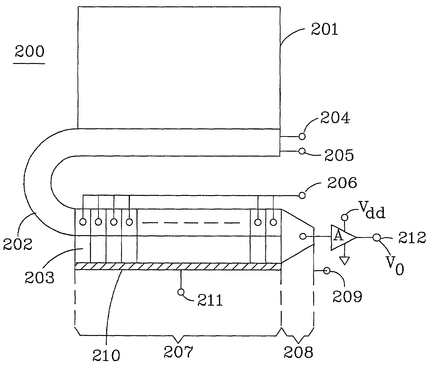
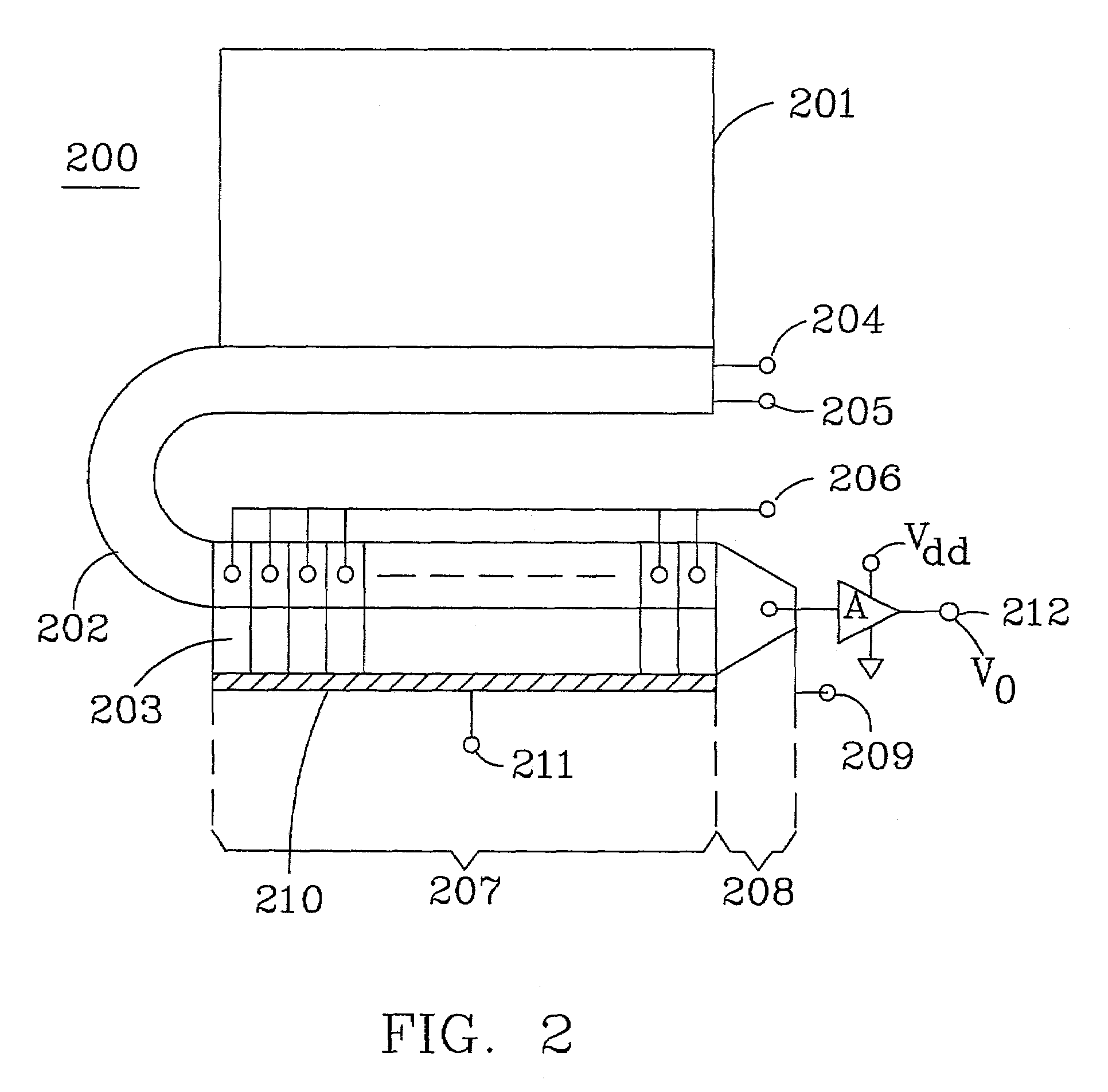
[0019]FIG. 2 shows a plan view of the CCD area image sensor 200 of the present invention. The sensor consists of an image sensing area 201 that interfaces with the extended serial register 202. Two-phase clocks applied to the terminal 204 and 205 clock serial register 202. The extended register 202 is coupled to the charge multiplication region 207 that consists of specially designed charge multiplication cells 203. The same clocks also clock this register, but additional charge multiplication gate is added that is clocked through the terminal 206. The charge multiplication region 207 essentially consists of two adjacent CCD registers coupled together in each cell by a charge overflow barrier. The charge summing and the charge detection node 208 that is reset by the reset clock applied to the terminal 209 terminates the multiplication region. The detected signal is buffered by an amplifier A, and delivered to the device output terminal 212. An antiblooming structure 210 may be inclu...


PUM


Abstract

A CCD device incorporates Charge Multiplication in its CCD registers together with charge domain Dynamic Range compression. This structure preserves the high dynamic range available in the charge domain of these devices, and avoids limiting it by an inadequate voltage swing of the charge detection nodes and amplifiers. The Dynamic Range compression is logarithmic from a predetermined built in threshold and noiseless. The technique has an additional advantage of maintaining the compact size of the registers, and the registers may also include antiblooming devices to prevent blooming.

Description

[0001]Priority is claimed from Provisional Application Ser. No. 60 / 295,424, filed Jun. 4, 2001.FIELD OF THE INVENTION[0002]The present invention relates to solid-state image sensors, and more specifically to image sensors that incorporate a Charge Multiplier (CM) in their structure.BACKGROUND OF THE INVENTION[0003]A typical image sensor senses light by converting impinging photons into electrons that are integrated (collected) in sensor pixels. After the integration cycle is completed, charge is converted into a voltage that is supplied to the output terminals of the device. The charge to voltage conversion is accomplished either directly in the sensor pixels, such as in the Active Pixel CMOS image sensors, or remotely off the sensing area in charge conversion amplifiers. In the remote conversion process, charge must be transported to the sensing amplifier by a well know charge transferring process using various vertical and horizontal Charge Coupled Device (CCD) registers.[0004]U.S...

Claims


Application Information

Patent Timeline
IPC IPC(8): H04N3/14H04N5/335H01L29/762H01L21/339H01L27/148H01L29/768H04N5/355H04N5/359H04N5/372H04N5/376
CPCH01L27/148H01L29/76816H01L27/14887H01L27/14812
Inventor HYNECEK, JAROSLAV
Owner ISETEX
Why Eureka
Try Eureka