
Semiconductor device for reducing coupling noise

a semiconductor and coupling noise technology, applied in the field of semiconductor devices, can solve the problems of increased manufacturing cost, read error, and read errors of flash memory, and achieve the effect of reducing or eliminating coupling noise and increasing chip area

Active Publication Date: 2007-03-13
SAMSUNG ELECTRONICS CO LTD
View PDF3 Cites 10 Cited by
  • Summary
  • Abstract
  • Description
  • Claims
  • Application Information

AI Technical Summary

Benefits of technology

This configuration effectively reduces or eliminates coupling noise between sense nodes without increasing chip area, thereby enhancing read operation accuracy and maintaining cost-effectiveness.

Problems solved by technology

Non-volatile memory does not lose data when power is lost, but is generally does not permit random access and is slower than volatile memory.
However, flash memory may have read errors due to coupling noise between sense lines of a page buffer.
Both of these solutions have the drawback of requiring increased memory chip size and / or increased manufacturing costs.
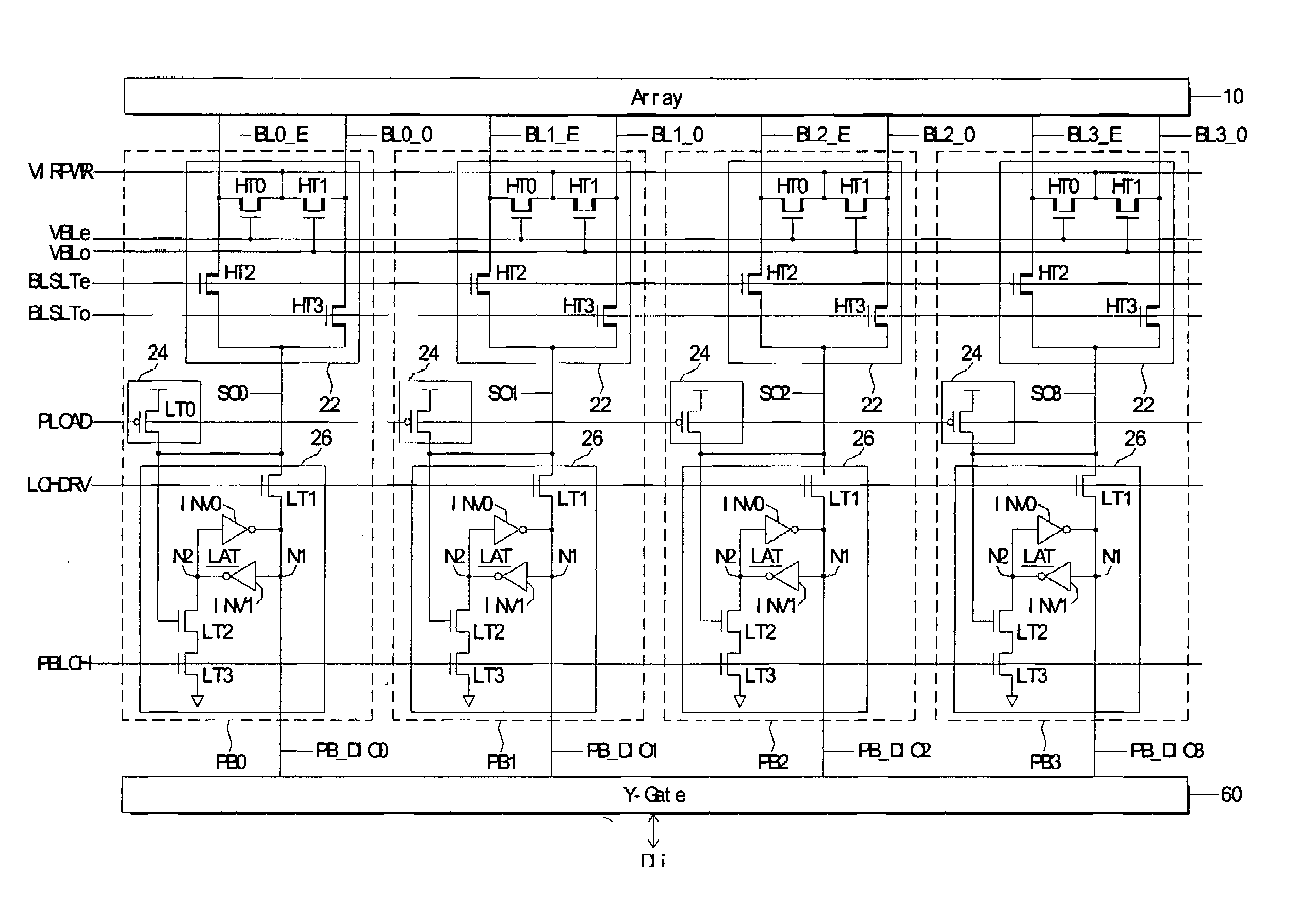
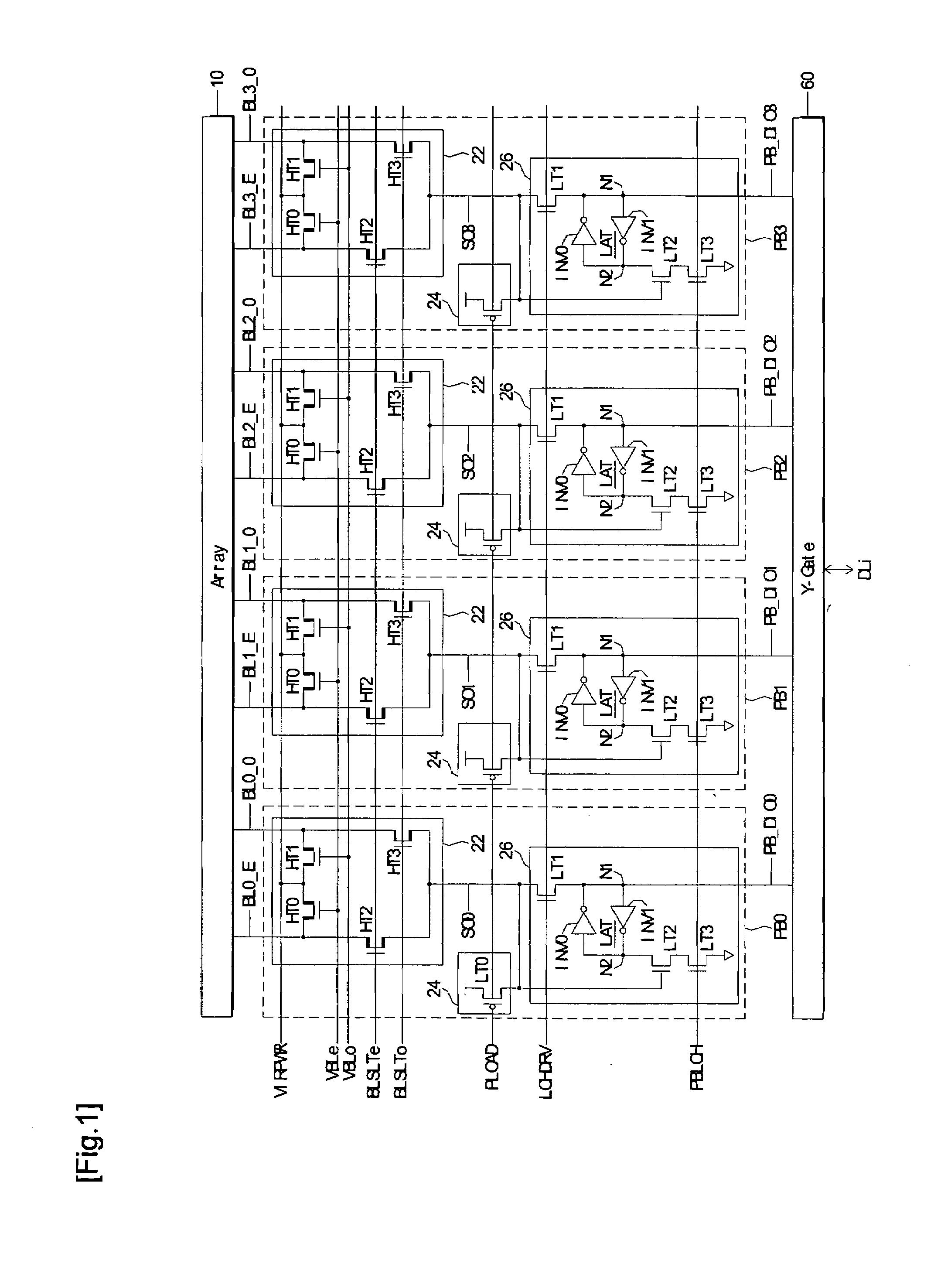
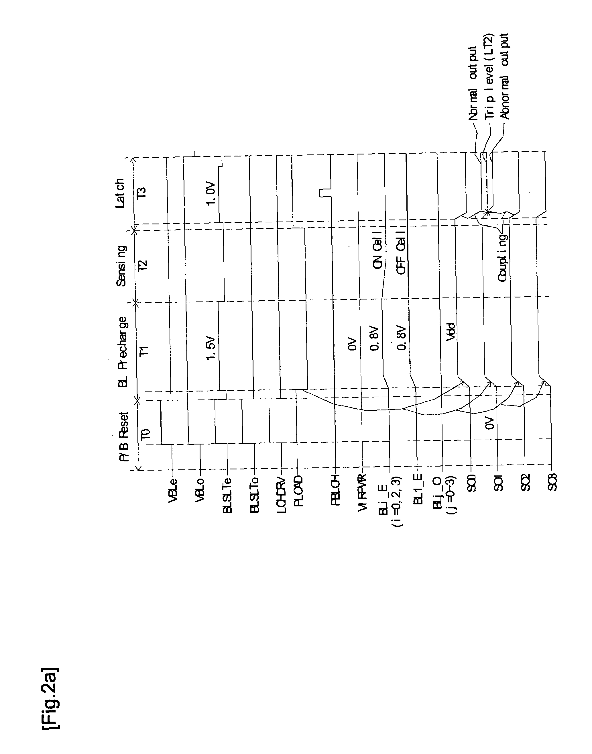
This layout may cause a read error, which is more clearly illustrated in FIG. 2a.
As a result, with a page buffer layout arrangement as shown in FIG. 2, a read error may be caused by the coupling noise between adjacent sense lines (or nodes).

Method used


Image

  • Semiconductor device for reducing coupling noise
  • Semiconductor device for reducing coupling noise
  • Semiconductor device for reducing coupling noise

Examples


Embodiment Construction

[0052]FIG. 3 illustrates a page buffer of a flash memory device according to an example embodiment of the present invention. As shown in FIG. 3, one more of the page buffers PB0, PB1, PB2, and PB3 of the present invention may include a switch transistor LT4. In FIG. 3, constituent elements that are identical to those in FIG. 1 are marked by the same reference numerals, and description thereof is thus omitted.

[0053]The switch transistor LT4 of each of page buffers PB0, PB1, PB2, and PB3 may be a low-voltage transistor, which is formed within a low-voltage region (or a low-voltage circuit region) where a pre-charge circuit 24 and a sense and latch circuit 26 of each page buffer PB0, PB1, PB2, and PB3 are formed. In each page buffer, a drain of the switch transistor LT4 may be electrically connected to a gate of an NMOS transistor LT2 as a sense transistor through a corresponding sense line SOi (i=0–3). A source of the switch transistor LT4 may be electrically connected to NMOS transis...


PUM


Abstract

Semiconductor devices, semiconductor memory device, or flash memories including a high voltage region including high voltage elements, a low voltage region including low voltage elements, and a switch transistor, such as a low voltage switch transistor, connecting the high voltage region and the high voltage region. The switch transistor reduces or eliminates coupling noise between sense nodes without increasing chip area.

Description

PRIORITY STATEMENT[0001]This application claims the benefit under 35 U.S.C. § 119(a) of Korean Patent Application No. 2004-020424, filed on Mar. 25, 2004, the contents of which are hereby incorporated by reference in their entirety.BACKGROUND OF THE INVENTION[0002]Recent developments in multimedia applications such as, cell phones, PDA, digital camera, etc. have increasingly required memory devices with higher density. Conventional memories include dynamic random access memory (DRAM), static random access memory (SRAM), and non-volatile memory (NVM). Non-volatile memory may include mask read only memory (ROM), electrically erasable programmable read only memory (EEPROM), and flash memory. Non-volatile memory does not lose data when power is lost, but is generally does not permit random access and is slower than volatile memory.[0003]Flash memory may be formed by a combination of erasable programmable read only memory (EPROM) and electrically erasable programmable read only memory (E...

Claims


Application Information

Patent Timeline
Patent Type & Authority Patents(United States)
IPC IPC(8): G11C11/34G11C7/18G11C5/06G11C16/04G11C16/26
CPCG11C16/26A63H33/22G02B27/08
Inventor BYEON, DAE-SEOK
Owner SAMSUNG ELECTRONICS CO LTD
Learn More