Read-only memory device coded with selectively insulated gate electrodes

a read-only memory and gate electrode technology, applied in semiconductor devices, semiconductor/solid-state device details, electrical apparatus, etc., can solve the problems of increasing the unit cost adding complexity and concomitant cost to the fabrication process, and affecting the quality of read-only memory chips, so as to achieve the effect of scaling down the size of the rom and broadening the process window

Active Publication Date: 2007-03-20
MACRONIX INT CO LTD
View PDF8 Cites 9 Cited by
  • Summary
  • Abstract
  • Description
  • Claims
  • Application Information

AI Technical Summary

Benefits of technology

[0011]The word lines contact and interconnect the gate electrodes corresponding to the active code positions, but the insulating layers prevent the word lines from contacting the gate electrodes of inactive code positions. Thus, the memory device is coded through the selective deposition of the insulating layers. As a result of ion implantation not being used for coding, the process window can be broadened and the size of the ROM can be scaled down. The memory device is then further metallized and encapsulated in a package.
[0012]Any feature or combination of features described herein are included within the scope of the present invention provided that the features included in any such combination are not mutually inconsistent as will be apparent from the context, this specification, and the knowledge of one of ordinary skill in the art. For purposes of summarizing the present invention, certain aspects, advantages and novel features of the present invention have been described herein. Of course, it is to be understood that not necessarily all such aspects, advantages or features will be embodied in any particular embodiment of the present invention. Additional advantages and aspects of the present invention are apparent in the following detailed description and claims.
[0010]The present invention addresses these needs by providing a semiconductor mask-programmable memory device coded by selective deposition of insulating layers on gate electrodes of the transistor memory cells of the device. The invention herein disclosed comprises a process for fabricating a memory device programmed with a binary code, and the resulting memory device. A dielectric layer is created on a surface of a semiconductor substrate. A plurality of substantially parallel strip-stacked layers is formed on the dielectric layer. Each strip-stacked layer comprises a polysilicon gate electrode layer on the dielectric layer, and a disposable silicon nitride layer disposed on the gate electrode layer. A plurality of source / drain regions is doped in the substrate adjacent to the surface. The source / drain regions are situated so that each strip-stacked layer is disposed substantially between a pair of adjacent source / drain regions. A plurality of first oxide spacers is deposited on the dielectric layer between the strip-stacked layers. The strip-stacked layers are patterned to form a plurality of polysilicon gate electrodes disposed on the dielectric layer and a plurality of disposable silicon nitride pillars disposed on the gate electrodes. Because portions of the strip-stacked layers are removed during the patterning of the strip-stacked layers, a plurality of trenches is created. The trenches are filled by forming a plurality of second oxide spacers, and the disposable pillars are removed to expose the polysilicon gate electrodes under them. A patterned mask is deposited on the memory device to cover the gate electrodes corresponding to active code positions of the memory device in accordance with the predetermined code, while leaving the inactive code positions exposed. Insulating silicon dioxide layers are then deposited on the exposed polysilicon gate electrodes through the openings in the mask, and the mask is removed. A conductive material is then deposited on the memory device and patterned into word lines perpendicular to the source / drain regions.
[0011]The word lines contact and interconnect the gate electrodes corresponding to the active code positions, but the insulating layers prevent the word lines from contacting the gate electrodes of inactive code positions. Thus, the memory device is coded through the selective deposition of the insulating layers. As a result of ion implantation not being used for coding, the process window can be broadened and the size of the ROM can be scaled down. The memory device is then further metallized and encapsulated in a package.
[0012]Any feature or combination of features described herein are included within the scope of the present invention provided that the features included in any such combination are not mutually inconsistent as will be apparent from the context, this specification, and the knowledge of one of ordinary skill in the art. For purposes of summarizing the present invention, certain aspects, advantages and novel features of the present invention have been described herein. Of course, it is to be understood that not necessarily all such aspects, advantages or features will be embodied in any particular embodiment of the present invention. Additional advantages and aspects of the present invention are apparent in the following detailed description and claims.

Problems solved by technology

The time required for ion implantation during the coding of a read-only memory chip device lengthens the total time required for the chip device fabrication, and thus increases the unit cost of the read-only memory chips.
Moreover, the ion implantation coding step adds complexity and concomitant cost to the fabrication process.
Furthermore, several diffusion-related problems may arise from the doping of the channel areas during ion implantation coding of the memory device.
Diffusion during ion implantation coding can make it relatively difficult to control the doped (implanted) area with a high degree of precision.
The presence of the dopant particles beyond the intended area may cause undesirable changes in the cell's performance, such as degradation of punch-through voltages between adjacent buried source / drain regions, and may also change the coding of adjacent cells.
Large size is, of course, the enemy of circuit miniaturization and unit cost.
Furthermore, the switching speed of circuits generally decreases with the increase in the size of individual transistors.

Method used


Image

  • Read-only memory device coded with selectively insulated gate electrodes
  • Read-only memory device coded with selectively insulated gate electrodes
  • Read-only memory device coded with selectively insulated gate electrodes

Examples


Embodiment Construction

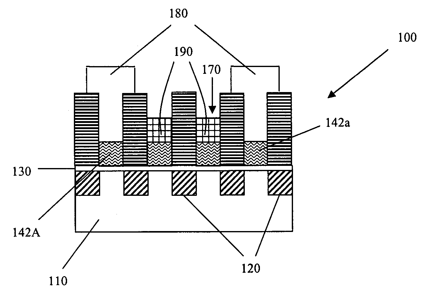
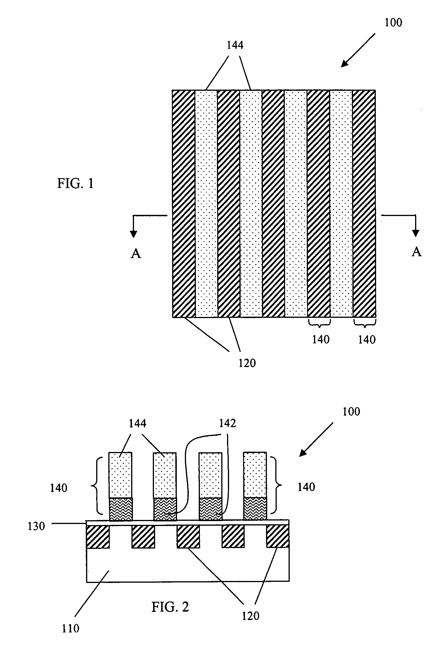
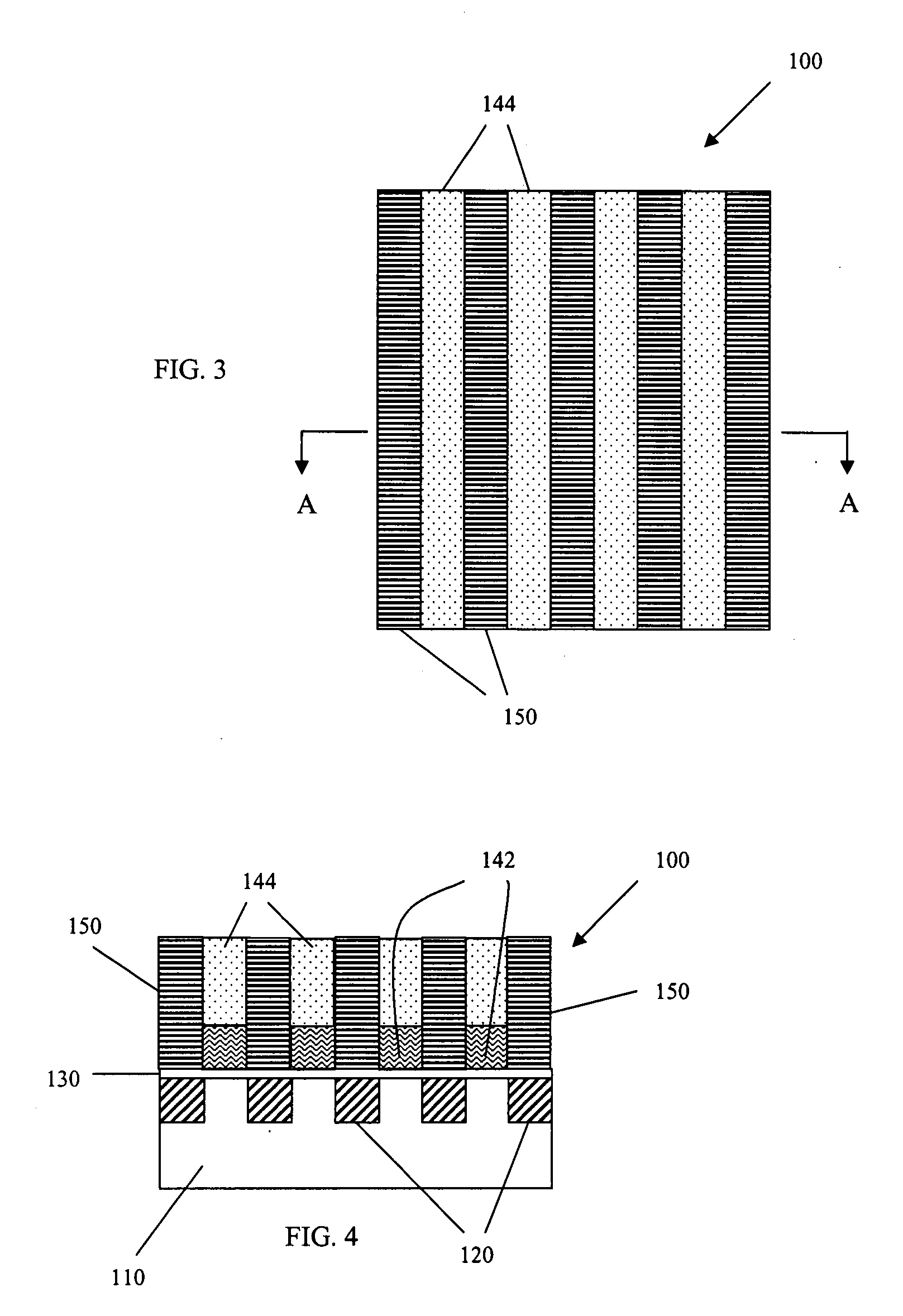
[0027]Reference will now be made in detail to the presently preferred embodiments of the invention, examples of which are illustrated in the accompanying drawings. Wherever possible, the same or similar reference numbers are used in the drawings and the description to refer to the same or like parts. It should be noted that the drawings are in simplified form and are not to precise scale. In reference to the disclosure herein, for purposes of convenience and clarity only, directional terms, such as top, bottom, left, right, up, down, over, above, below, beneath, rear, and front are used with respect to the accompanying drawings. Such directional terms should not be construed to limit the scope of the invention in any manner.

[0028]Although the disclosure herein refers to certain illustrated embodiments, it is to be understood that these embodiments are presented by way of example and not by way of limitation. The intent of the following detailed description, although discussing exemp...


PUM


Abstract

During fabrication of a mask read-only memory (ROM) device, a dielectric layer is grown on a substrate. Strip-stacked layers are formed on the dielectric layer, with each strip-stacked layer including a polysilicon and a silicon nitride layer. Source / drain regions are formed in the substrate between the strip-stacked layers, and spacers are then deposited between the strip-stacked layers. The strip-stacked layers are patterned into gates, which are disposed over every code position, with silicon nitride pillars being disposed on the gates. Additional spacers are formed on gate sidewalls. The silicon nitride pillars are removed, exposing the gates. A mask is then formed to cover active code positions, in accordance with the desired programming code. Insulating layers are then deposited through the mask onto the exposed gates. When the mask is removed, word lines are formed, interconnecting the gates without the insulating layers.

Description

BACKGROUND OF THE INVENTION[0001]1. Field of the Invention[0002]The present invention relates generally to semiconductor fabrication methods and, more particularly, to semiconductor mask-programmable read-only memory devices and methods for fabrication of such devices.[0003]2. Description of Related Art[0004]As the information revolution continues to unfold, the numbers and capabilities of computers and of other digital systems continue to increase. One of the common, and essential, elements of a typical digital system is memory. Consequently, the need for ever-faster, denser, and less expensive memories remains unabated.[0005]Computer memories are generally of two kinds: random access memories, or RAMs; and read-only memories, or ROMs. Data can be written into a random access memory and read from it with equal ease. Data can also be read from a read-only memory in the course of normal operation. But, as the name “read-only memory” implies, data is either not written into a read-onl...

Claims


Application Information

Patent Timeline
Patent Type & Authority Patents(United States)
IPC IPC(8): H01L21/82H01L21/8239H01L21/8246H01L27/10H01L27/112H01L31/0328
CPCH01L27/11253H01L27/112H10B20/00H10B20/38
Inventor YANG, CHUN-YI
Owner MACRONIX INT CO LTD
Why Eureka
Try Eureka