Fully silicided NMOS device for electrostatic discharge protection

a technology of nmos and shielding device, which is applied in the direction of transistors, basic electric elements, electric devices, etc., can solve the problems of reducing the protection performance of ggnmos device, reducing ics being susceptible to damage, so as to improve the esd protection performance, reduce the depletion barrier, and improve the effect of esd characteristics

Inactive Publication Date: 2007-04-17
CHARTERED SEMICONDUCTOR MANUFACTURING
View PDF14 Cites 41 Cited by
  • Summary
  • Abstract
  • Description
  • Claims
  • Application Information

AI Technical Summary

Benefits of technology

[0013]Another object of the present invention is to provide a semiconductor device that provides electrostatic discharge (ESD) protection without requiring additional processing steps.
[0014]Another object of the present invention is to provide a semiconductor device that provides electrostatic discharge (ESD) protection that does not require the salicidation blocking step.
[0015]Another object of the present invention is to provide a semiconductor device that provides electrostatic discharge (ESD) protection that does not require an additional implantation to improve ESD characteristics.
[0016]A still further object of the present invention is to provide a semiconductor device that provides electrostatic discharge (ESD) protection having a trigger point away from the semiconductor surface.
[0017]These objects are achieved using a process where n-wells are added below the source and drain regions in a GGNMOS device. The n-well and p-well doping profiles are tailored such that the peaks of the well concentrations occur away from the silicon surface. This reduces the depletion barrier between the p-well and n-well source. In addition, the increased electric field between the reverse biased n-well drain and p-well will result in higher electron-hole generation current. This injects more holes into the p-well producing a potential that will forward bias the p-well / n-well source junction. The result is effectively a bipolar NPN transistor that is conducting. Low resistance between the drain and source quickly removes any electrostatic charge. The conduction occurs away from the silicon surface where power may be effectively dissipated.

Problems solved by technology

Integrated circuits (ICs) are susceptible to damage from a phenomenon called electrostatic discharge (ESD).
If not properly controlled, ESD will irreparably damage the IC as power dissipated during the discharge yields large temperature gradients within the device structure.
Unfortunately, the salicidation reduces the ESD protection performance of a GGNMOS device due to discharge current localization.
Soft breakdown is the phenomenon where conduction results from excessive generation of electron-hole pairs.
If the electric field reaches a critical level where hard breakdown occurs, a small increase in drain voltage will cause a very large increase in current.
This occurs because the two depletion regions described above are moved closer to each other, resulting in significant field penetration from the drain to the source.
Further increase of VDS will cause the depletion regions to touch resulting in punch through.

Method used


Image

  • Fully silicided NMOS device for electrostatic discharge protection
  • Fully silicided NMOS device for electrostatic discharge protection
  • Fully silicided NMOS device for electrostatic discharge protection

Examples


Embodiment Construction

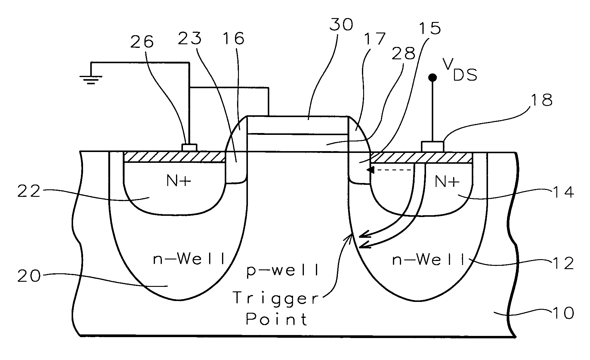
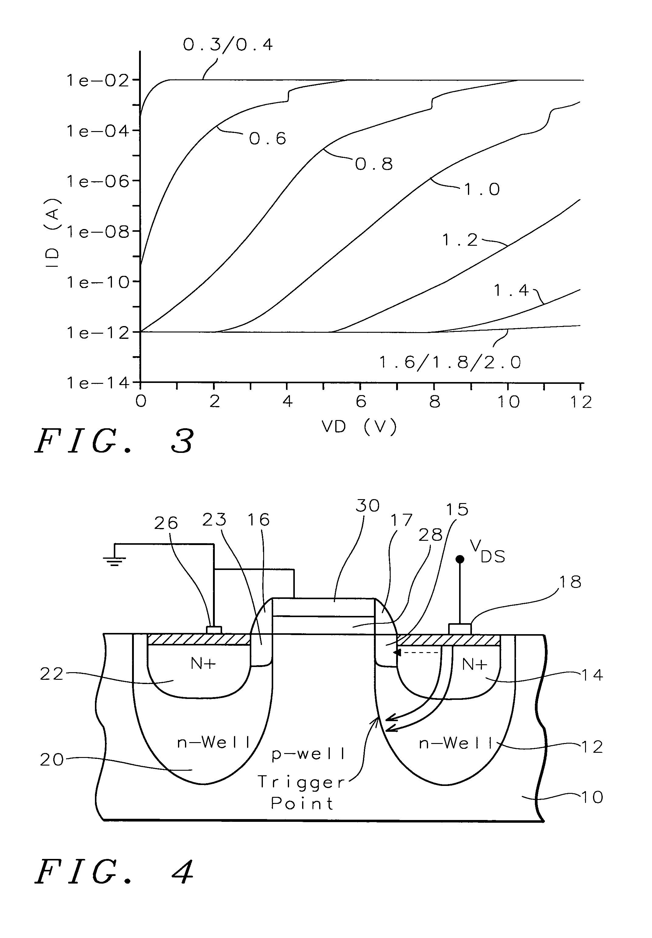
[0026]The present invention uses a method of ESD protection using a grounded gate NMOS (GGNMOS) device to provide the low resistance discharge path. N-wells are added below the source and drain regions of a GGNMOS device in order to tailor the doping profiles of those regions. Snapback is used to provide ESD protection. As VDS increases, the potential barrier at the n-well source is lowered due to the DIBL effect. Generation of electron-hole pairs in the drain well depletion region also occurs. This generation current dominates and increases with VDS. This results in a higher electric field and higher electron-hole generation current. The hole current will be injected into the p-well, forward biasing the p-well / n-well source junction. The DIBL effect aids this by lowering the potential barrier at the n-well source. Once the p-well / n-well source junction is forward biased, the device behaves as an NPN transistor where the drain acts as the collector. A low resistance discharge path i...


PUM


Abstract

A device and method are described for forming a grounded gate NMOS (GGNMOS) device used to provide protection against electrostatic discharge (ESD) in an integrated circuit (IC). The device is achieved by adding n-wells below the source and drain regions. By tailoring the dopant concentration profiles of the p-well and n-wells provided in the fabrication process, peak dopant concentrations are moved below the silicon surface. This moves ESD conduction deeper into the IC where thermal conductivity is improved, thereby avoiding thermal damage occurring with surface conduction. The device does not require a salicidation block or additional implantation and uses standard NMOS fabrication processing steps, making it advantageous over prior art solutions.

Description

[0001]This is a division of patent application Ser. No. 10 / 170,248, filing date Jun. 12, 2002 now U.S. Pat. No. 6,830,966, Fully Silicided Nmos Device For Electrostatic Discharge Protection, assigned to the same assignee as the present invention, which is herein incorporated by reference in its entirety.BACKGROUND OF THE INVENTION[0002](1) Field of the Invention[0003]The invention generally relates to the fabrication of semiconductor devices and, more particularly, to a method of forming an NMOS device for electrostatic discharge (ESD) protection in the fabrication of integrated circuits.[0004](2) Description of Prior Art[0005]Integrated circuits (ICs) are susceptible to damage from a phenomenon called electrostatic discharge (ESD). ESD occurs during transportation and handling of the device when large static charges collect on their external pins. If not properly controlled, ESD will irreparably damage the IC as power dissipated during the discharge yields large temperature gradien...

Claims


Application Information

Patent Timeline
Patent Type & Authority Patents(United States)
IPC IPC(8): H01L23/62H01L29/72H01L29/74H01L31/111H01L31/119H01L21/336H01L21/76H01L21/8234H01L23/60H01L27/02H01L29/08H01L29/10H01L29/76H01L29/78H01L31/062
CPCH01L27/0266H01L29/0847H01L29/1083Y10S257/90H01L29/7833
Inventor CAI, JUNLO, KENG FOO
Owner CHARTERED SEMICONDUCTOR MANUFACTURING
Why Eureka
Try Eureka