Anisotropic dry etching of Cu-containing layers

a technology of anisotropic dry etching and cu-containing layers, applied in the field of semiconductor processing, can solve the problems of difficult difficult scratching of cmp, and difficulty in defining extremely fine features

Inactive Publication Date: 2007-05-08
TOKYO ELECTRON LTD
View PDF19 Cites 9 Cited by
  • Summary
  • Abstract
  • Description
  • Claims
  • Application Information

AI Technical Summary

Benefits of technology

[0013]The above and other objects are achieved, according to the present invention, by providing a method and an apparatus that uses a directional beam of high kinetic energy (hyperthermal) neutral O-atoms to anisotropically oxidize Cu layers, and an etching gas comprising an etch reagent that readily reacts with the oxidized Cu layers to form volatile Cu-containing etch products. The high directionality of the O-atom beam allows for anisotropic etching of the Cu layers in accordance with a patterned hard mask or photoresist.

Problems solved by technology

However, Cu CMP technology is challenging and it has difficulty defining extremely fine features.
In addition, CMP suffers from yield-detracting problems of scratching, peeling, dishing and erosion.
While ion bombardment is needed to achieve the desired degree of etch anisotropy, it is also responsible for secondary damage to the underlying microstructure.
As semiconductor devices have become increasingly more integrated and new advanced materials, such as copper and low-k dielectric materials, have been introduced to improve the circuit properties, the damage caused by fabrication processes presents an increasingly serious problem.
The Cu removal rates are very low when using this method and another drawback is that the sputtered CuClx coats the chamber walls and this requires periodic cleaning of the etching chamber.
An equally serious problem is encountered when high-aspect-ratio features are etched in chlorine plasma and the sputtered CuClx products redeposit on the feature sidewalls where the effects of physical sputtering are reduced.
When the abovementioned chlorine-based etching process is carried out at elevated temperatures (>200° C.) to increase the volatility of the reacted Cu-containing layer, corrosion can occur due to the accumulated CuClx etch residues on the surface.
If these residues are not removed by a post-etch cleaning step, they can cause continuing corrosion of the Cu even after the application of a protective layer over the etched features.
However, these approaches are not practical for semiconductor batch processing of large substrates due to poor etch uniformity, high cost and added equipment complexity, and reliability problems.
Such particles are ordinarily required to achieve an isotropic etch with atomic oxygen plasmas in the prior art, but cause secondary damage to the underlying substrate.
Furthermore, the reaction products should be highly volatile and easily removed from the etched substrate.
In addition, the aforementioned limitations that are encountered when etching Cu-containing layers using conventional chlorine chemistry, show that there is a need for new low temperature dry etching methods in semiconductor manufacturing using chemical approaches that do not involve chlorine-based reactants.

Method used


Image

  • Anisotropic dry etching of Cu-containing layers
  • Anisotropic dry etching of Cu-containing layers
  • Anisotropic dry etching of Cu-containing layers

Examples


Embodiment Construction

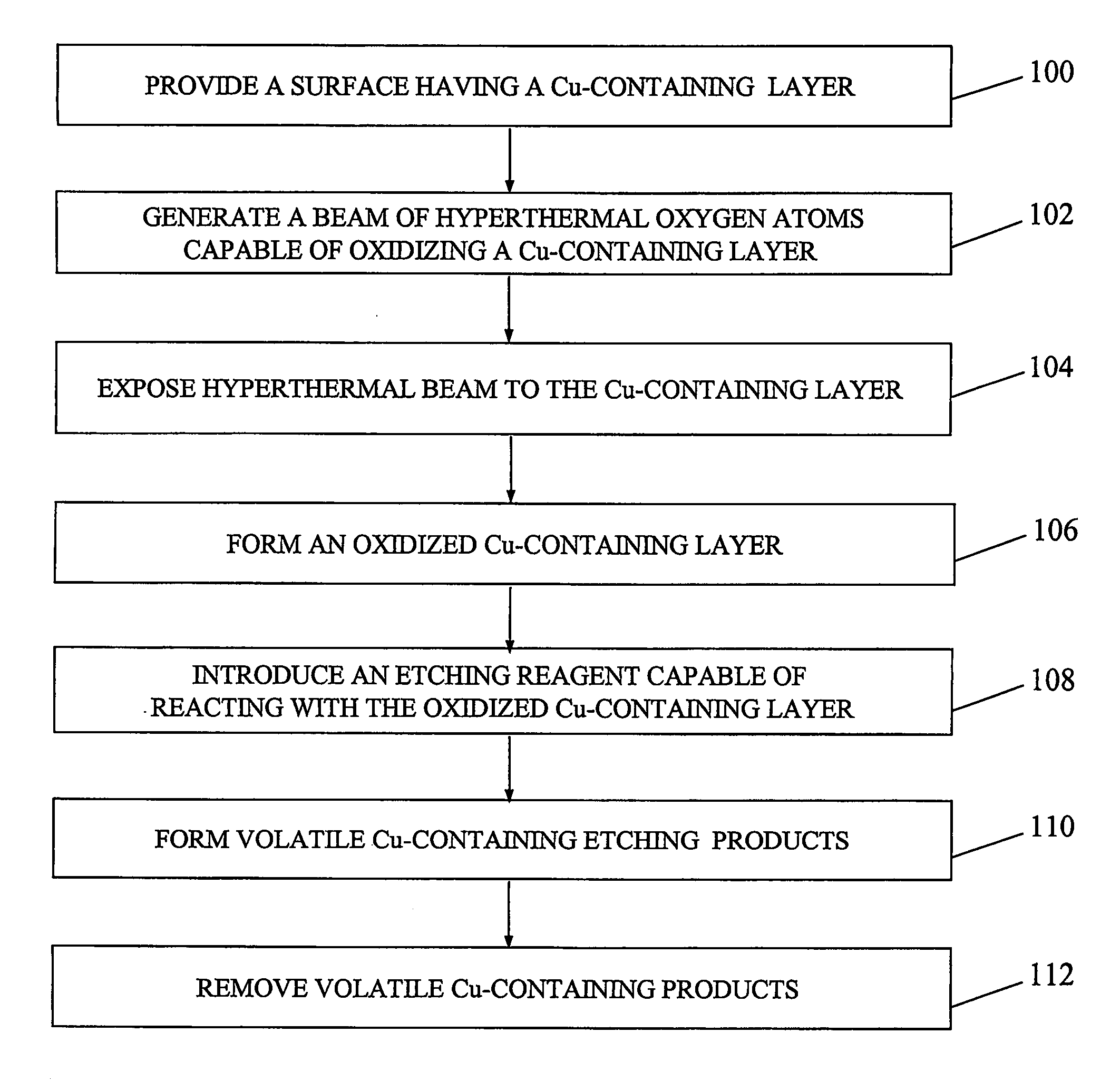
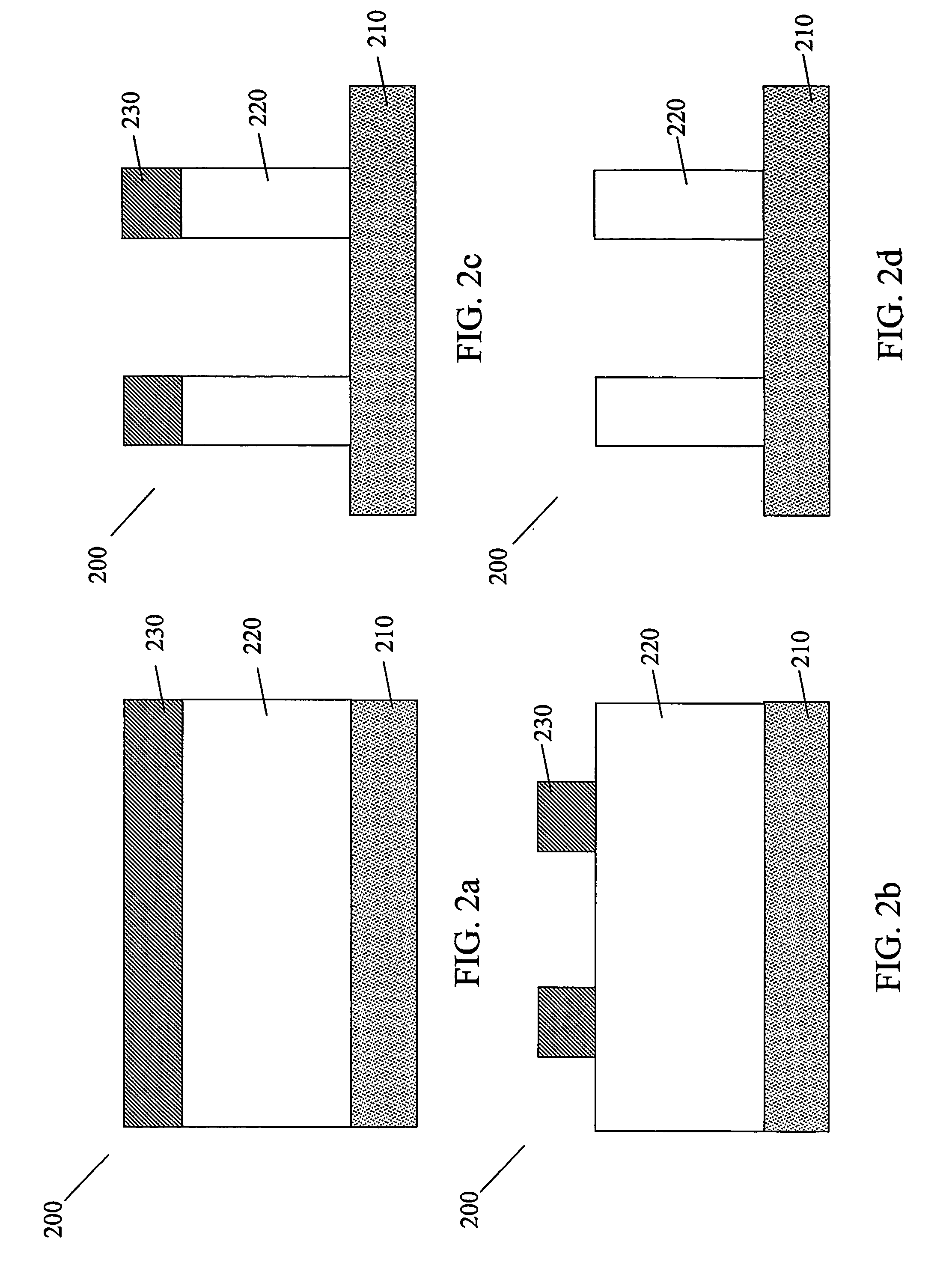
[0021]In general, the present invention pertains to a method and an apparatus for etching pure Cu and Cu-containing layers in manufacturing integrated circuits. The method uses a directional beam of high kinetic energy O-atoms to oxidize the Cu layers, and an etch reagent that forms volatile Cu-containing etch products when reacted with the oxidized Cu layers.

[0022]Importantly, the etch reagent reacts very slowly with unoxidized Cu on feature sidewalls, but reacts readily with oxidized Cu surfaces at low temperatures. Therefore, in order to achieve anisotropic etching and avoid undercutting of etch features, the oxidation rate of Cu on the vertical sidewalls of the etch features must be substantially slower than the oxidation of Cu on the horizontal surfaces. This is achieved using a directional O-atom beam.

[0023]The directional beam is preferably a hyperthermal beam of neutral O-atoms that has high kinetic energy and can be produced with low divergence from the substrate normal, th...


PUM

PropertyMeasurementUnit
temperatureaaaaaaaaaa

Abstract

A method and apparatus for dry etching pure Cu and Cu-containing layers (220, 310) for manufacturing integrated circuits. The invention uses a directional beam of O-atoms with high kinetic energy (340) to oxidize the Cu and Cu-containing layers, and etching reagents (370) that react with the oxidized Cu (360) to form volatile Cu-containing etch products (390). The invention allows for low-temperature, anisotropic etching of pure Cu and Cu-containing layers in accordance with a patterned hard mask or photoresist (230, 330).

Description

CROSS-REFERENCE TO RELATED APPLICATIONS[0001]This application claims priority to U.S. Provisional Application Ser. No. 60 / 392,045, filed Jun. 28, 2002; and is related to co-pending Provisional Application Ser. No. 60 / 379,754 filed on May 14, 2002, the entire contents of which are incorporated herein by reference.FIELD OF THE INVENTION[0002]The present invention relates to the field of semiconductor processing and more particularly to a method and apparatus for anisotropic etching and patterning of pure Cu and Cu-containing layers used in integrated circuits.BACKGROUND OF THE INVENTION[0003]Copper (Cu) is emerging as the metal of choice in a wide variety of semiconductor applications. Lower electrical resistivity, coupled with improved electromigration performance and increased stress migration resistance are important material properties that favor the use of Cu over aluminum (Al) in interconnect lines and contacts. The lower electrical resistance is critical since it allows signals...

Claims


Application Information

Patent Timeline
Patent Type & Authority Patents(United States)
IPC IPC(8): C23F1/02B44C1/22B81C1/00C23F1/00C23F1/12C23F4/00H01L21/3213H01L21/768
CPCB81C1/00492C23F1/12C23F4/00H01L21/32135H01L21/32136H01L21/76838B81C2201/0143
Inventor CHEN, LEELUDVIKSSON, AUDUNN
Owner TOKYO ELECTRON LTD
Why Eureka
Try Eureka