Semiconductor device including fuse elements and bonding pad

Active Publication Date: 2007-05-15
RENESAS ELECTRONICS CORP
View PDF5 Cites 4 Cited by
  • Summary
  • Abstract
  • Description
  • Claims
  • Application Information

AI Technical Summary

Benefits of technology

[0012]Therefore, the present invention proposes an improved semiconductor device and a method for manufacturing such a

Problems solved by technology

However, since Cu has, higher melting point and boiling point than Al, blowing using conventional YAG or YLF laser is difficult, and when a conventional blowing method is used, it is difficult that a Cu wiring is used as a fuse.
It is also difficult to perform Au or Al wire bonding on a Cu wiring, and Al is generally used for the uppermost wiring layer that forms the portion used as the bonding pad.
On the other hand, since a silicon nitride film absorbs much laser beams, and has a high melting point, the blow of the Al wiring in the silicon nitride film may produce blow residues, and cannot be performed properly.
Therefore, when a silicon nitride film is used as the passivation film, it is difficult to use the Al wiring in the up

Method used


Image

  • Semiconductor device including fuse elements and bonding pad
  • Semiconductor device including fuse elements and bonding pad
  • Semiconductor device including fuse elements and bonding pad

Examples


Example

First Embodiment

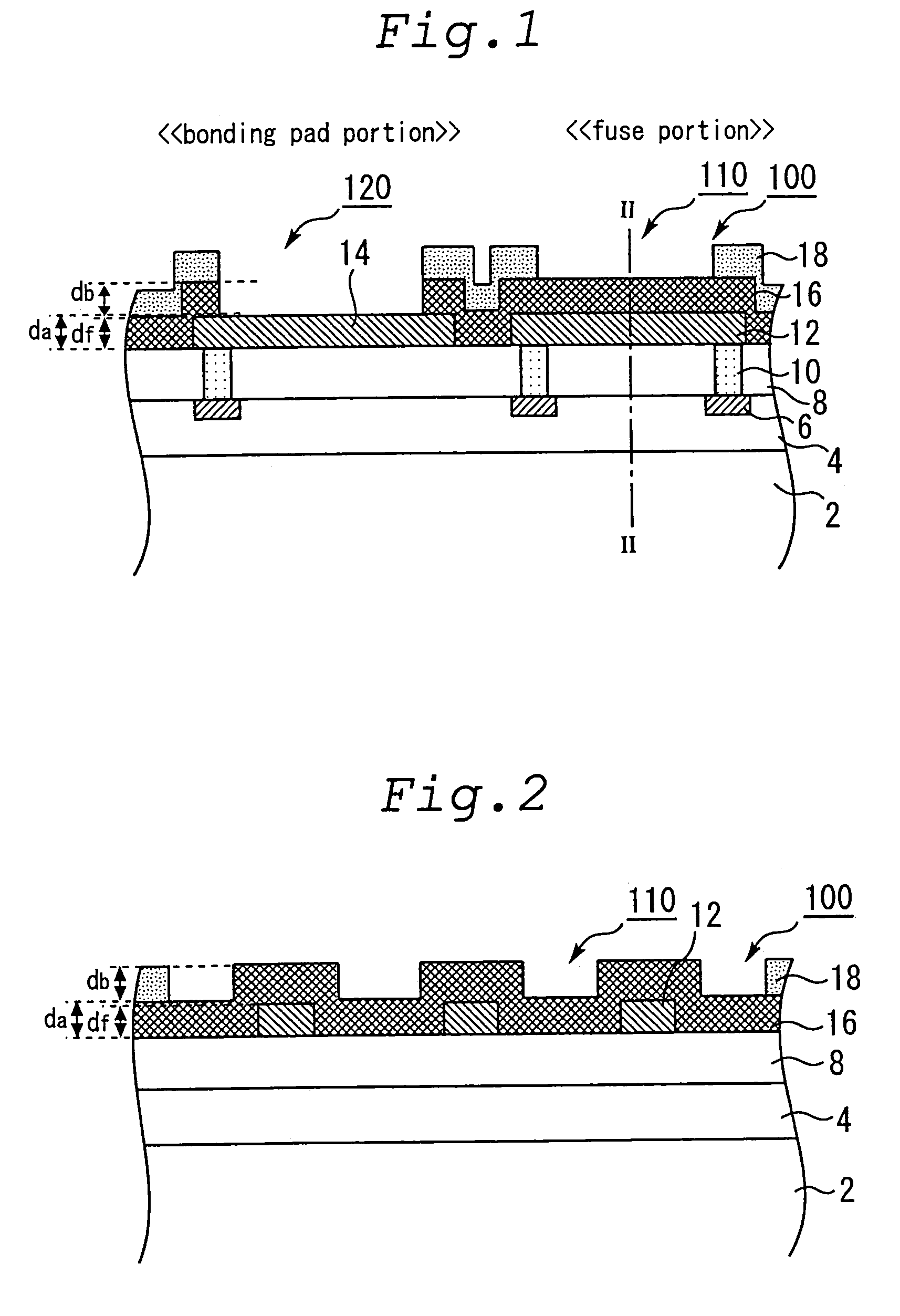
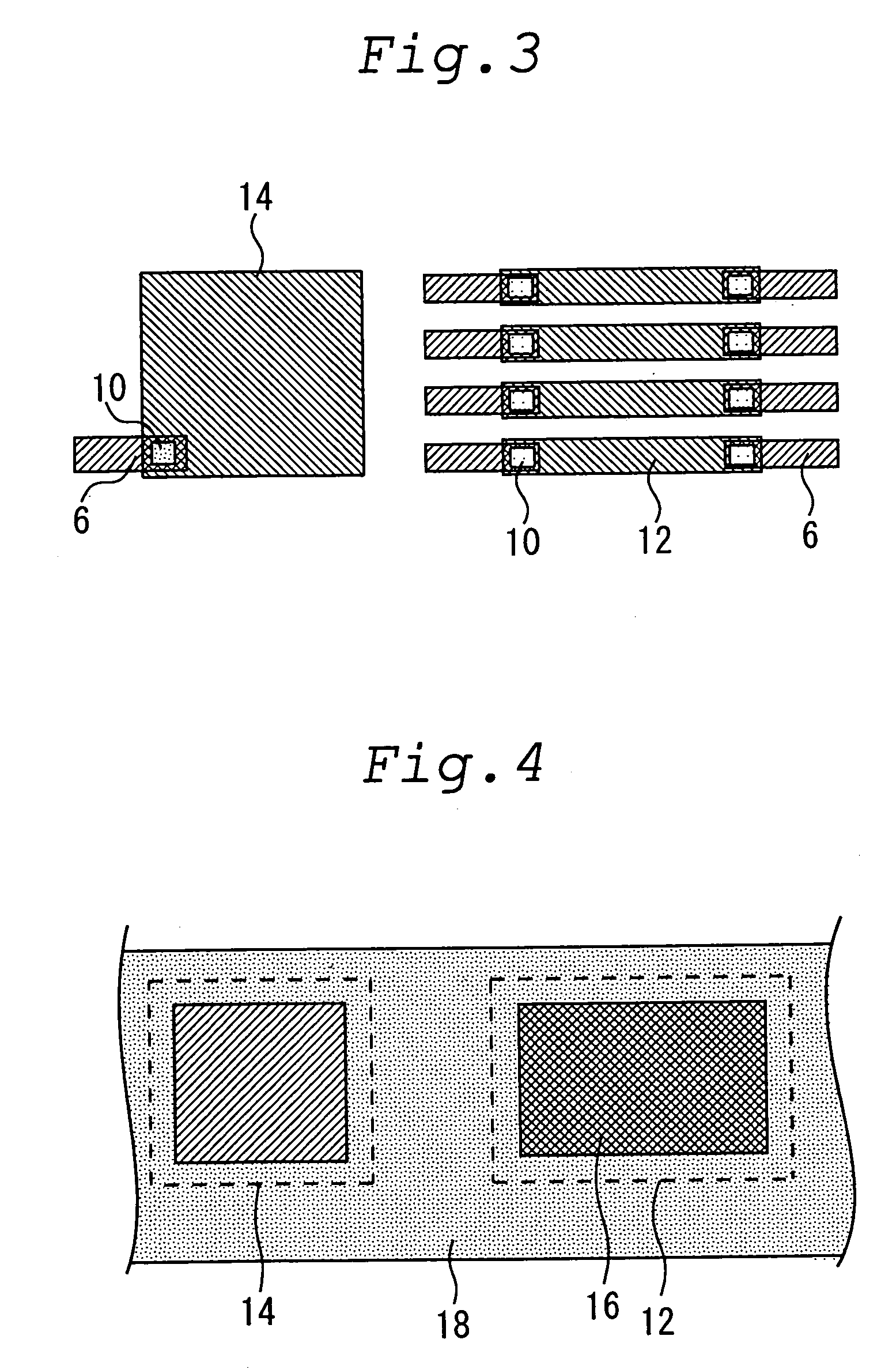
[0042]FIG. 1 is a schematic sectional view for illustrating the structure of a semiconductor device 100 in the first embodiment of the present invention. FIG. 2 is a schematic sectional view in the II—II direction of the semiconductor device 100 in FIG. 1. FIG. 3 is a schematic perspective top view of the wiring layers of the semiconductor device 100, and

[0043]FIG. 4 is a schematic top view of the semiconductor device 100. As FIGS. 1 and 2 show, in the semiconductor device 100, an interlayer insulating film 4 is formed on an Si substrate 2, and Cu wirings 6 are formed in the interlayer insulating film 4. An interlayer insulating film 8 is formed on the surfaces of the Cu wirings 6, and on the exposing surface of the interlayer insulating film 4. Via holes 10 that pass through the interlayer insulating film 8 are formed in the locations of the interlayer insulating film 8 corresponding to the locations of the Cu wirings 6, and are filled with tungsten.
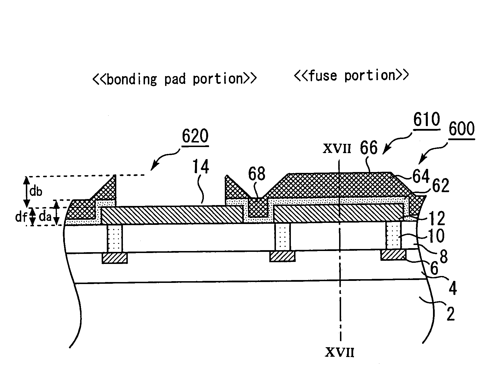
[0044]The fuse p...

Example

[0063]Also in the first embodiment 1, there was described the case where the silicon oxide film 16 and the silicon nitride film 18 are formed using a P-CVD method. However, the present invention is not limited to the use of a P-CVD method, but these may be formed using other methods.

Example

Second Embodiment

[0064]FIG. 6 is a schematic sectional view for illustrating a semiconductor device 200 in the second embodiment of the present invention. FIG. 7 is a schematic diagram showing the cross section of the semiconductor device 200 in FIG. 6 in the VII—VII direction.

[0065]As FIGS. 6 and 7 show, the semiconductor device 200 resembles the semiconductor device 100. Also in the semiconductor device 200, an interlayer insulating film 4 is formed on an Si substrate 2, Cu wirings 6 are buried on the interlayer insulating film 4, furthermore, an interlayer insulating film 8 is formed on the interlayer insulating film 4 and the Cu wirings 6, and via holes 10 filled with tungsten are formed in the interlayer insulating film 8. Also in the fuse portion 210, a fuse wiring 12 is formed, and in the bonding pad portion 220, a bonding pad 14 is formed. The fuse wiring 12 and the bonding pad 14 has the same thickness df as in the first embodiment.

[0066]As in the semiconductor device 100, ...


PUM


Abstract

A semiconductor device includes a lower-layer substrate, a fuse above the lower-layer substrate and blown by radiation with light, a silicon oxide film on the fuse and on an exposed portion of the surface of the lower-layer substrate, and a silicon nitride film on the silicon oxide film. The portion of the silicon oxide film on the surface of the lower-layer substrate is thicker than the fuse, and the silicon oxide film has an opening opposite the fuse.

Description

BACKGROUND OF THE INVENTION[0001]1. Field of the Invention[0002]The present invention relates to a semiconductor device. More specifically, the present invention relates to a semiconductor device having a portion used as a fuse.[0003]2. Background Art[0004]In recent years, accompanying the miniaturization, and increase in the capacity and speed of semiconductor devices, a rescuing method for securing the yield is taken in a semiconductor manufacturing process wherein spare memory cells are previously prepared in a semiconductor device, and when a defective bit is found, the defective bit is replaced by a spare memory cell. As the method for replacing the defective bit to a spare memory cell, a method wherein the portion to be used as a fuse is previously provided in a wiring layer, and a program to blow the fuse, whereby to transmit a signal to use the spare memory cell, is provided.[0005]As a method to blow the fuse, the laser trimming system wherein laser beams are radiated onto t...

Claims


Application Information

Patent Timeline
IPC IPC(8): H01L27/10H01L21/3205H01L21/768H01L21/82H01L23/52H01L23/522H01L23/525
CPCH01L23/5258H01L24/05H01L24/03H01L2224/05554H01L24/45H01L2224/04042H01L2224/05082H01L2224/05624H01L2224/45124H01L2224/45144H01L2224/48624H01L2224/48724H01L2924/01013H01L2924/01014H01L2924/01015H01L2924/01022H01L2924/01029H01L2924/0105H01L2924/01073H01L2924/01074H01L2924/01079H01L2924/01082H01L2924/04953H01L2924/05042H01L2224/05553H01L2224/02166H01L2924/01033H01L2924/01006H01L24/48H01L2924/00014H01L2924/12042H01L2924/00
Inventor FUJIKI, NORIAKIYAMASHITA, TAKASHIIZUMITANI, JUNKO
Owner RENESAS ELECTRONICS CORP
Why Eureka
Try Eureka