CMOS image sensor and method for manufacturing the same

a technology of image sensor and manufacturing method, which is applied in the direction of electrical equipment, semiconductor devices, radio frequency controlled devices, etc., can solve the problems of high power consumption, complicated manufacturing process, and complicated drive mode, and achieve the effect of restricting the increase of dark current of the cmos image sensor

Inactive Publication Date: 2007-05-15
CONVERSANT INTPROP MANAGEMENT INC
View PDF16 Cites 28 Cited by
  • Summary
  • Abstract
  • Description
  • Claims
  • Application Information

AI Technical Summary

Benefits of technology

[0019]Accordingly, the present invention has been made to solve the above-mentioned problem(s), and an object of the present invention is to improve device characteristics of a CMOS image sensor by preventing impurities from being ion-implanted to the boundary portion between an isolation layer and an active region for a photodiode, thus reducing dark current.
[0029]Accordingly, the present invention is provided so that the passivation layer (a laminate structure generally the same as the transistor gate structure) is formed on an edge portion of the active region for the photodiode, and is used as a masking layer against an ion implantation. The result is a photodiode diffusion region spaced apart from the isolation layer, which prevents damage by ion implantation of impurities into the boundary portion (or interface) between the isolation layer and the photodiode diffusion region, and which restricts an increase of dark current of the CMOS image sensor.

Problems solved by technology

The CCD has various disadvantages, such as a complicated drive mode, high power consumption, a complicated manufacturing process derived from a relatively high number of photolithographic process steps and so forth.
Additionally, the CCD has a disadvantage in that it is difficult to make a product compact, due to difficulty in integrating various circuits such as a controlling circuit, a signal processing circuit, analog / digital converting circuit and so on into a chip for the CCD.
The conventional CMOS image sensor 100 with such construction may suffer from degradations of device performance and electric charge storing capacity, due to an increase of dark current.
Dark current may cause considerable problems such as degradations of performance and electric charge storing capacity in the CMOS image sensor under low illumination conditions.
However, the conventional CMOS image sensor has been greatly affected by dark current generated at the boundary portions of the isolation region and the P0 type diffusion region, and the P0 type diffusion region the n− type diffusion region.
Consequently, such defects can increase leakage current of the photodiode and therefore dark current of the CMOS image sensor.
Thus, the conventional CMOS image sensor has a limit in increasing performance characteristics of the device because it is difficult to restrict dark current generated at the boundary portion between the isolation layer and the active region for the photodiode, and to maintain device characteristics between the pixels constant.
Meanwhile, Korean Laid-Open Patent Publication Nos. 2001-61349, 2001-61353 and 2003-52639 disclose a method for reducing dark current of CMOS image sensor, which, however, do not present a solution to restrict an increase of dark current by preventing impurities from being ion-implanted to the boundary portion between an isolation layer and an active region for a photodiode.

Method used


Image

  • CMOS image sensor and method for manufacturing the same
  • CMOS image sensor and method for manufacturing the same
  • CMOS image sensor and method for manufacturing the same

Examples


Embodiment Construction

[0038]Hereinafter, a preferred embodiment of the present invention will be described with reference to the accompanying drawings. In the following description and drawings, the same reference numerals are used to designate the same or similar components, and so repetition of the description of the same or similar components will be omitted.

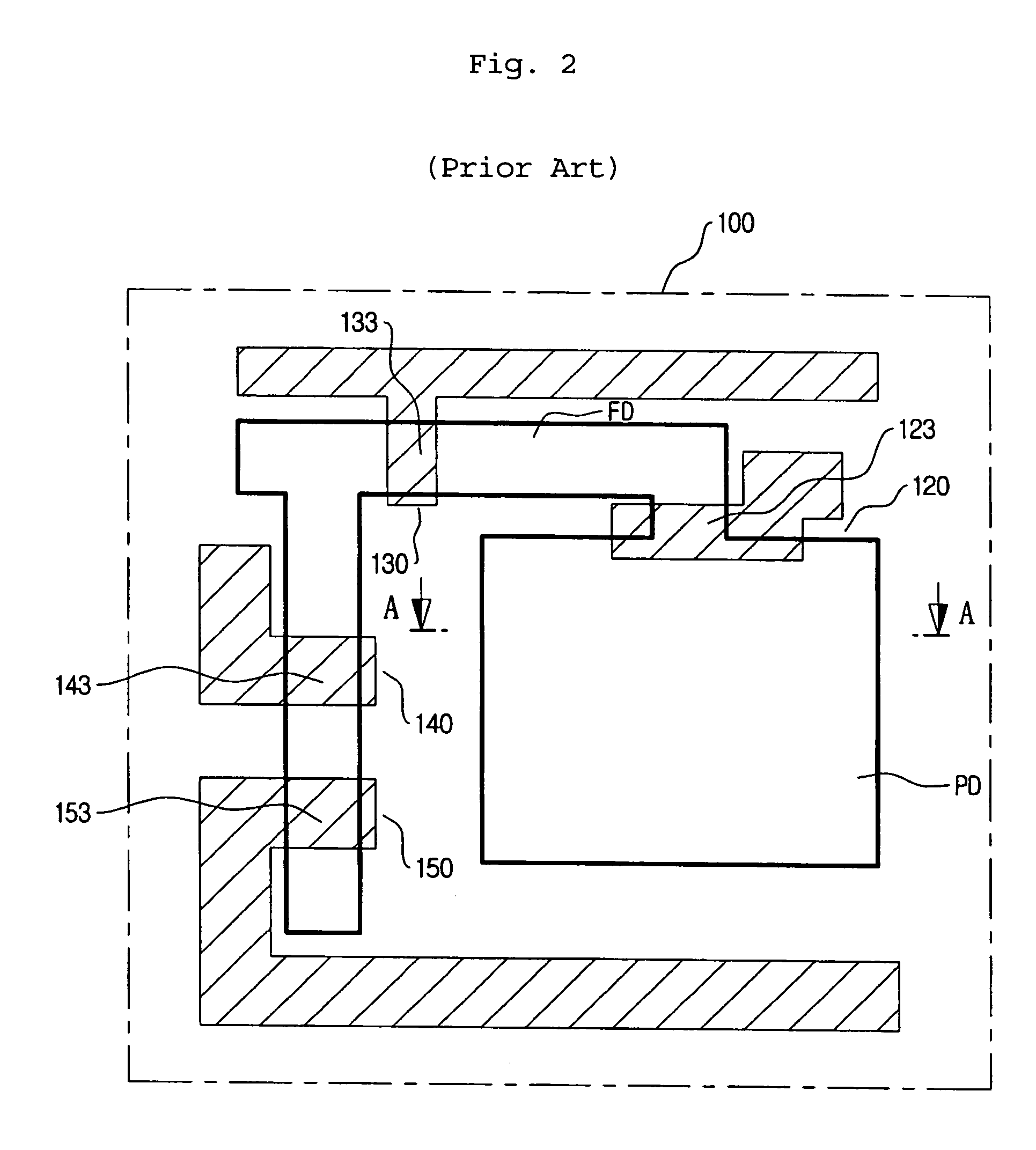
[0039]FIG. 4 is a layout of a unit pixel of a CMOS image sensor of the present invention.

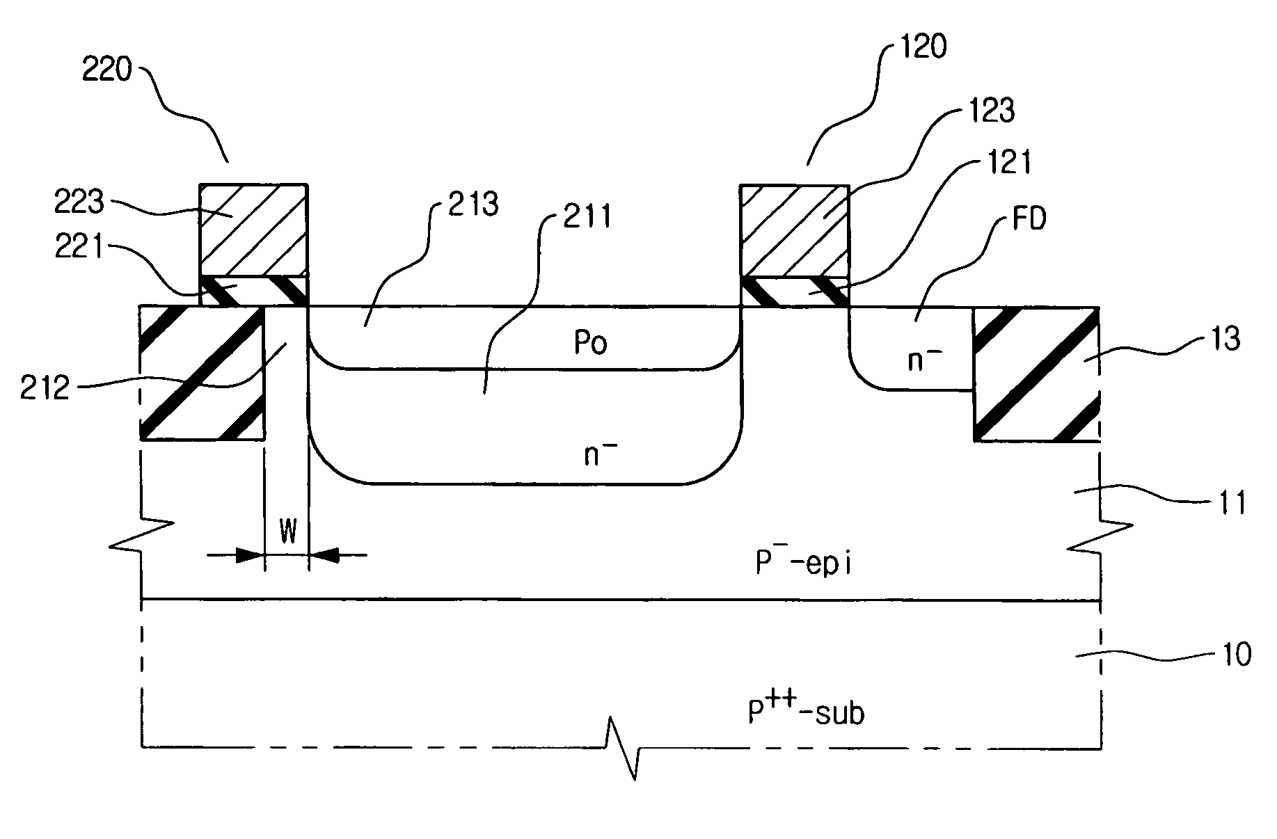
[0040]Referring to FIG. 4, in a unit pixel 200 of a CMOS image sensor of the present invention, an active region is a region defined by a bold solid line and an isolation region is a region outside the active region in which an isolation layer (not shown) is formed. The gates 123, 133, 143 and 153, respectively of the transfer transistor 120, reset transistor 130, drive transistor 140 and select transistor 150 are disposed as to be across an upper portion of the active region.

[0041]Furthermore, in order to prevent an edge portion of the active region for the p...


PUM


Abstract

A CMOS image sensor and a manufacturing method thereof are disclosed. The gates of the transistors are formed in an active region of a unit pixel, and at the same time, a passivation layer is formed on an edge portion of the active region of a photodiode to have the same laminate structure as the gates of the transistors. Impurities for a diffusion region of the photodiode are ion-implanted into the active region for the photodiode, after the laminate structure is formed. The passivation layer prevents the edge portion from being damaged by ion implantation at the boundary or interface between the photodiode diffusion region and an isolation layer, which reduces dark current and / or leakage current of the CMOS image sensor.

Description

BACKGROUND OF THE INVENTION[0001]1. Field of the Invention[0002]The present invention relates to a CMOS image sensor, and more particularly to a CMOS image sensor and method for manufacturing the same, in which a diffusion region of a photodiode is disposed apart from an isolation layer, and thereby a dark current is reduced.[0003]2. Description of the Prior Art[0004]In general, an image sensor is a semiconductor device for converting an optical image into an electrical signal, and is generally classified into a charge coupled device (CCD) and a complementary MOS (CMOS) image sensor.[0005]The CCD is a device constructed in such a manner that each MOS capacitor is adjacently disposed to each other, and that charge carriers are stored on any one of the MOS capacitors and then transferred to another MOS capacitor next to the MOS capacitor that stores the charge carrier. The CCD has various disadvantages, such as a complicated drive mode, high power consumption, a complicated manufactur...

Claims


Application Information

Patent Timeline
Patent Type & Authority Patents(United States)
IPC IPC(8): H01L27/148H01L21/00H01L27/14H01L27/146H01L31/00
CPCH01L27/14603H01L27/14609H01L27/1463H01L27/146
Inventor HAN, CHANG HUN
Owner CONVERSANT INTPROP MANAGEMENT INC
Why Eureka
Try Eureka