Nanoelectronic devices and circuits
- Summary
- Abstract
- Description
- Claims
- Application Information
AI Technical Summary
Benefits of technology
Problems solved by technology
Method used
Image


Examples
Embodiment Construction
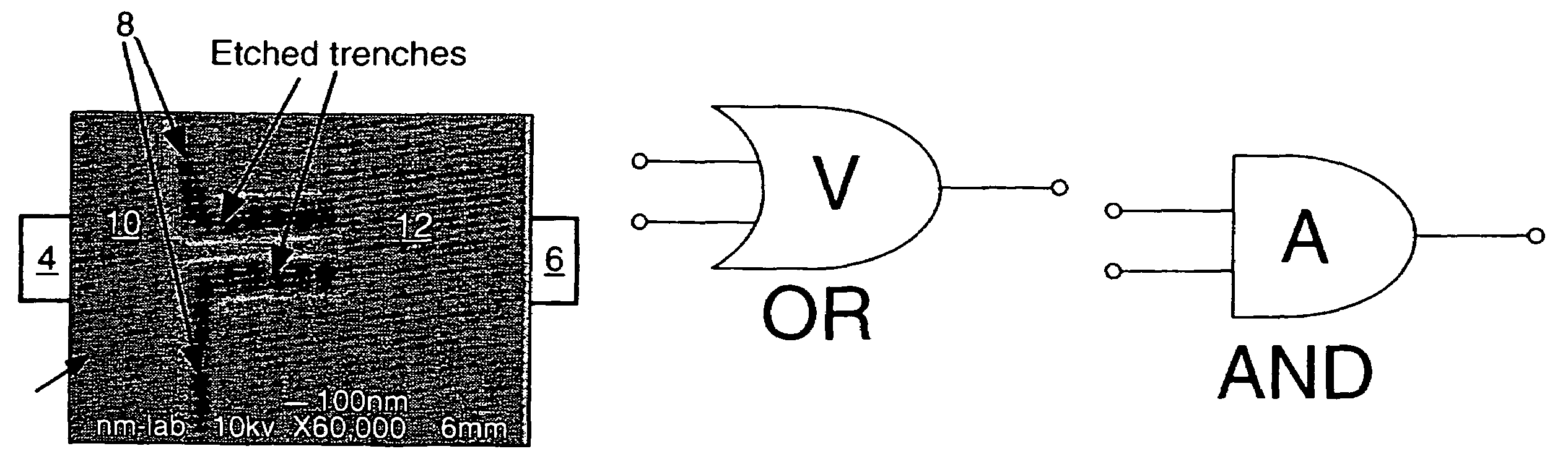
[0031]The roadmap of micro-electronics has long indicated that we will very soon reach the limits of conventional semiconductor devices, and near future integrated circuits must be built with nanodevices based on new concepts. Furthermore, it is highly desirable that these new nanodevices can be made on standard silicon wafers. Despite great efforts in making nanodevices working at room temperature, there is very little success. The reason is that most nanodevices proposed so far require a feature size of about a few nm.
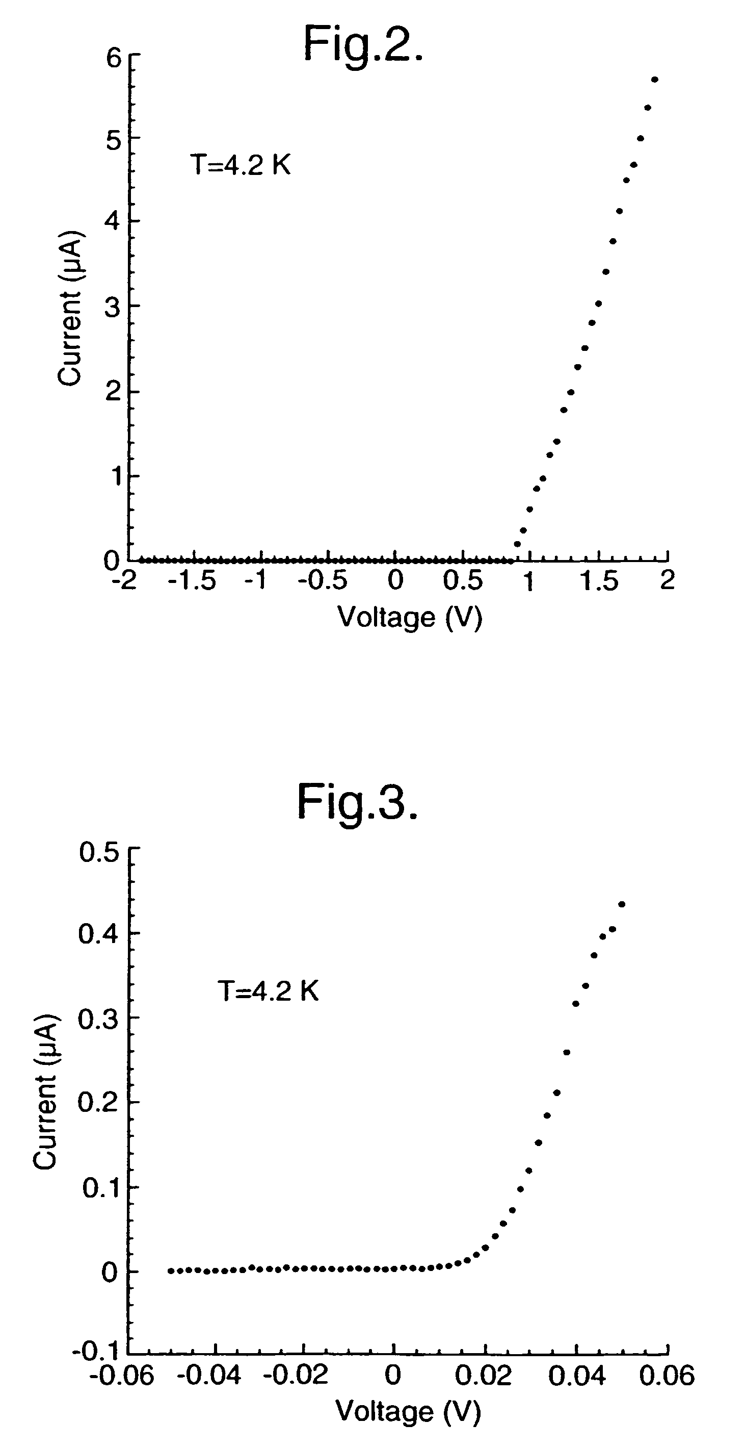
[0032]The invention includes diode-type devices. The current-voltage characteristic of the diode-like devices is just like that of a conventional diode, but both the threshold voltage (from 0V to a few volts) and the current level (from nA to μA) can be tuned by orders of magnitude by simply changing the device geometry, with no need to change the property of the host material by doping, diffusion, etc. Better than a pn diode, the leakage current under the backward b...
PUM
 Abstract
Description
Claims
Application Information