Interface circuit
- Summary
- Abstract
- Description
- Claims
- Application Information
AI Technical Summary
Benefits of technology
Problems solved by technology
Method used
Image

Examples
first embodiment
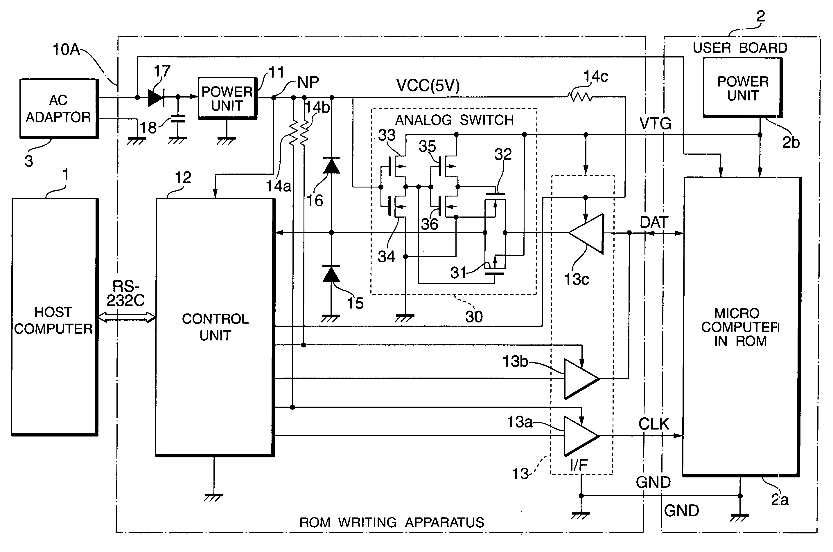
[0043]FIG. 1 is a constructional diagram of a ROM writing system showing the first embodiment of the invention, in which component elements which are common to those in FIG. 2 are designated by the same reference numerals.
[0044]According to the ROM writing system, in a manner similar to the ROM writing system of FIG. 2, a program or data which is sent from the host computer 1 is written into the flash memory built in the microcomputer 2a on the user board 2 and the system has a ROM writing apparatus 10A. The host computer 1 and the ROM writing apparatus 10A are connected by, for example, the serial interface of the RS-232C standard. The ROM writing apparatus 10A is connected to the terminal on the side of the user board 2 via the probe cable.
[0045]The ROM writing apparatus 10A has the power unit 11 which receives a voltage of 12V (DC) which is supplied from the AC adapter 3 via a diode 17 for preventing a reverse current and a capacitor 18 for smoothing and generates the stable powe...
second embodiment
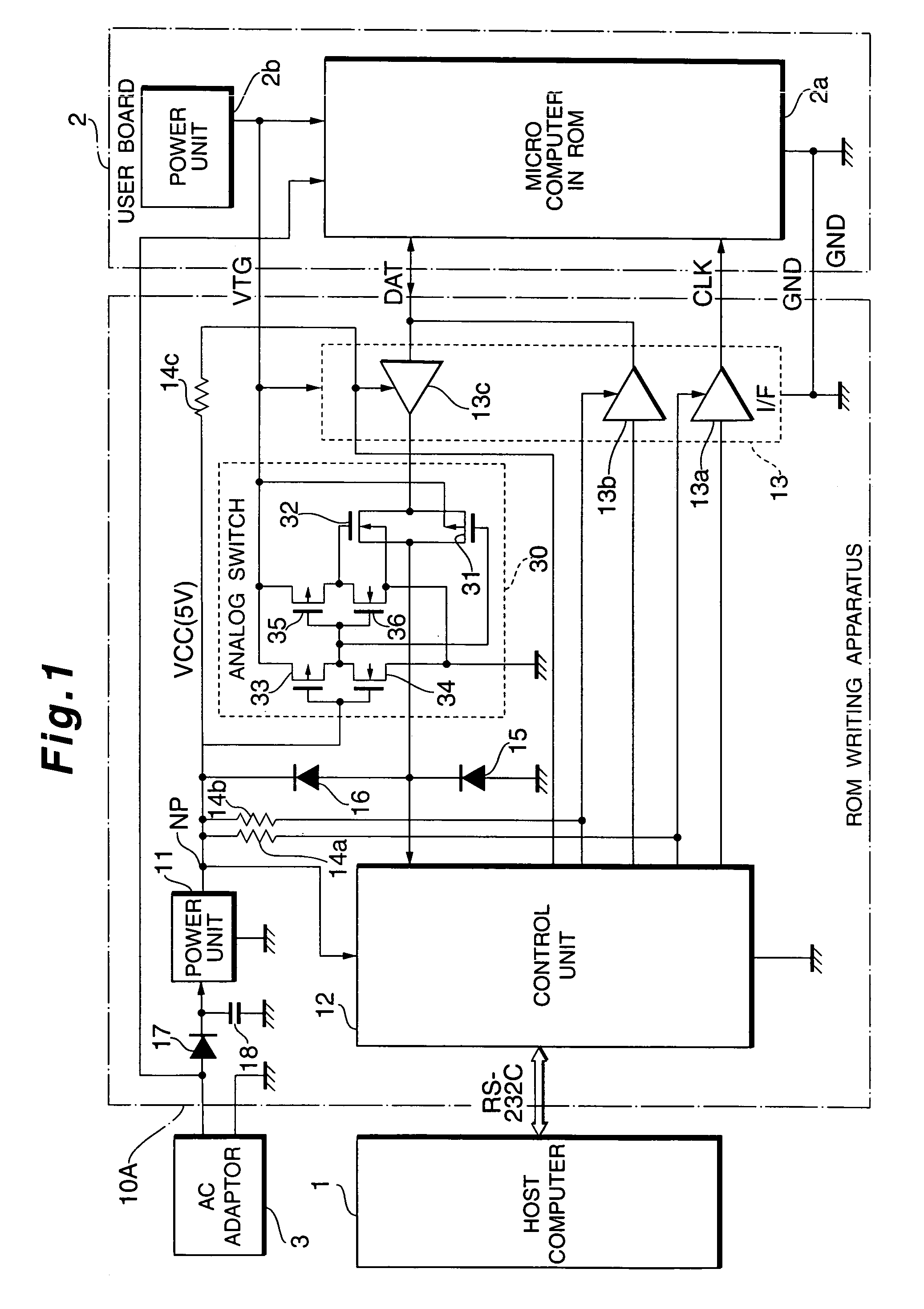
[0060]FIG. 4 is a constructional diagram of an interface circuit showing the second embodiment of the invention. In FIG. 4, component elements which are common to those in FIG. 1 are designated by the same reference numerals.
[0061]In a manner similar to, for example, the ROM writing system of FIG. 1, the interface circuit of FIG. 4 is provided to transmit and receive signals between the first apparatus (for example, ROM writing apparatus) and the second apparatus (for example, user board) which have different power sources, respectively.
[0062]The interface circuit has the power unit 11 which receives a DC voltage supplied from an AC adaptor (not shown) via the diode 17 for preventing a reverse current and the capacitor 18 for smoothing and forms the stable power voltage VCC. An output side of the power unit 11 is connected to the power node NP and the power voltage VCC is applied from the power node NP to a logic circuit 19.
[0063]Further, the interface circuit has the 3-state buffer...
third embodiment
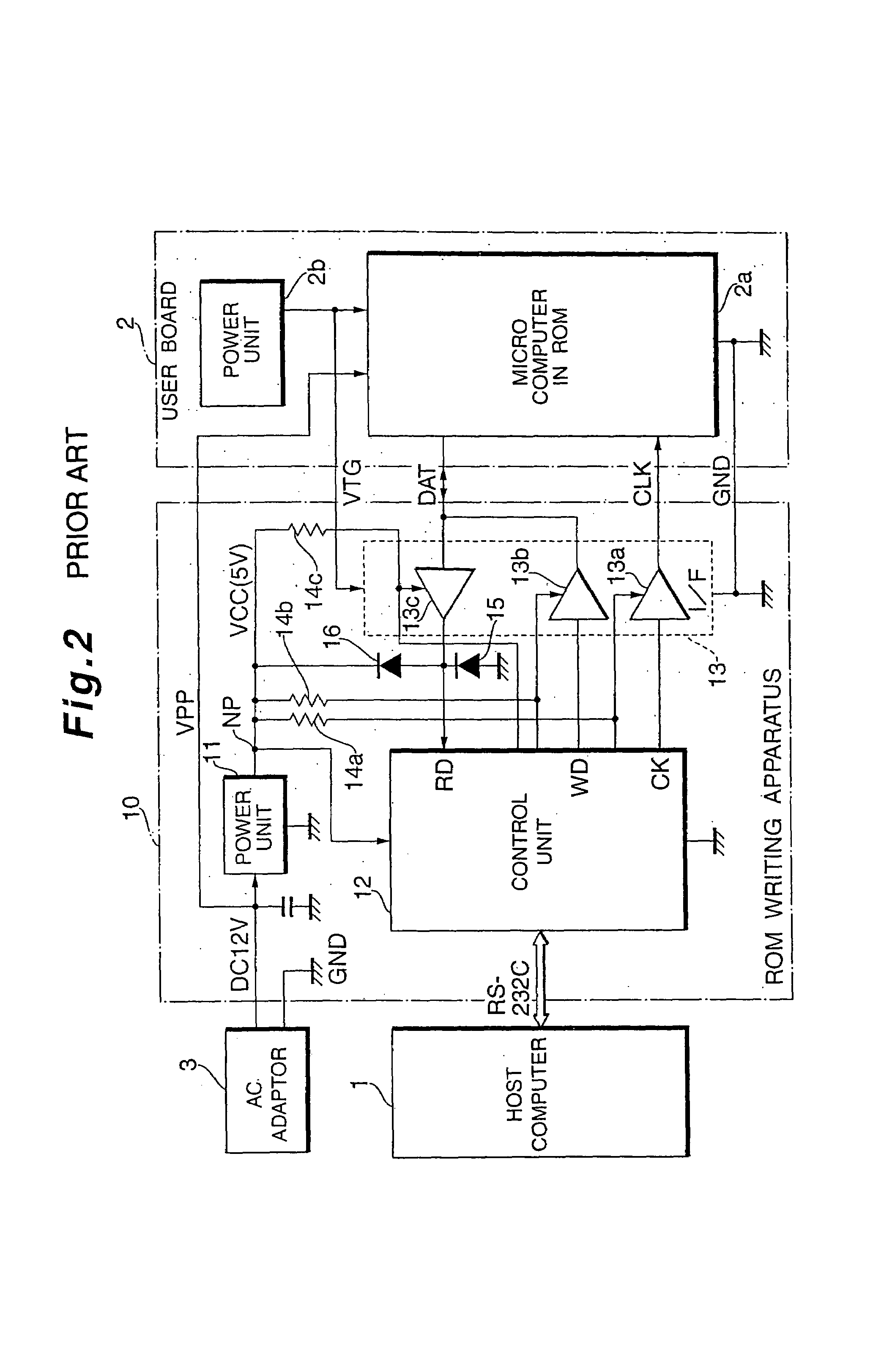
[0072]FIG. 5 is a constructional diagram of an interface circuit showing the third embodiment of the invention, in which component elements which are common to those in FIG. 4 are designated by the same reference numerals.
[0073]According to the interface circuit, the analog switch 30 in FIG. 4 is deleted, the output side of the 3-state buffer 13c is directly connected to the control unit 12, and an analog switch 30A is inserted between the pull-up resistor 14c and the control terminal of the 3-state buffer 13c. The analog switch 30A is driven by the power voltage VTG which is applied from the second apparatus side and on / off-controlled by the output signal of the voltage detector 40. Other constructions are similar to those in FIG. 4.
[0074]Subsequently, the operation will be described.
[0075]When the power voltage VTG is applied from the second apparatus side, the 3-state buffer 13c and the analog switch 30A are driven. When the DC voltage is supplied from the AC adaptor, the power v...
PUM
 Abstract
Description
Claims
Application Information
 - R&D Engineer
- R&D Manager
- IP Professional
- Industry Leading Data Capabilities
- Powerful AI technology
- Patent DNA Extraction
Browse by: Latest US Patents, China's latest patents, Technical Efficacy Thesaurus, Application Domain, Technology Topic.
© 2024 PatSnap. All rights reserved.Legal|Privacy policy|Modern Slavery Act Transparency Statement|Sitemap