

Substrate processing method
a technology of nitridation method and oxide film, which is applied in the direction of basic electric elements, electrical equipment, semiconductor devices, etc., can solve the problems of increasing the current through the oxide film, increasing the defect rate of the dielectric film, and cvd nitride film generally having a large number of defects
- Summary
- Abstract
- Description
- Claims
- Application Information
AI Technical Summary
Benefits of technology
Problems solved by technology
Method used
Image

Examples
first embodiment
[First Embodiment]
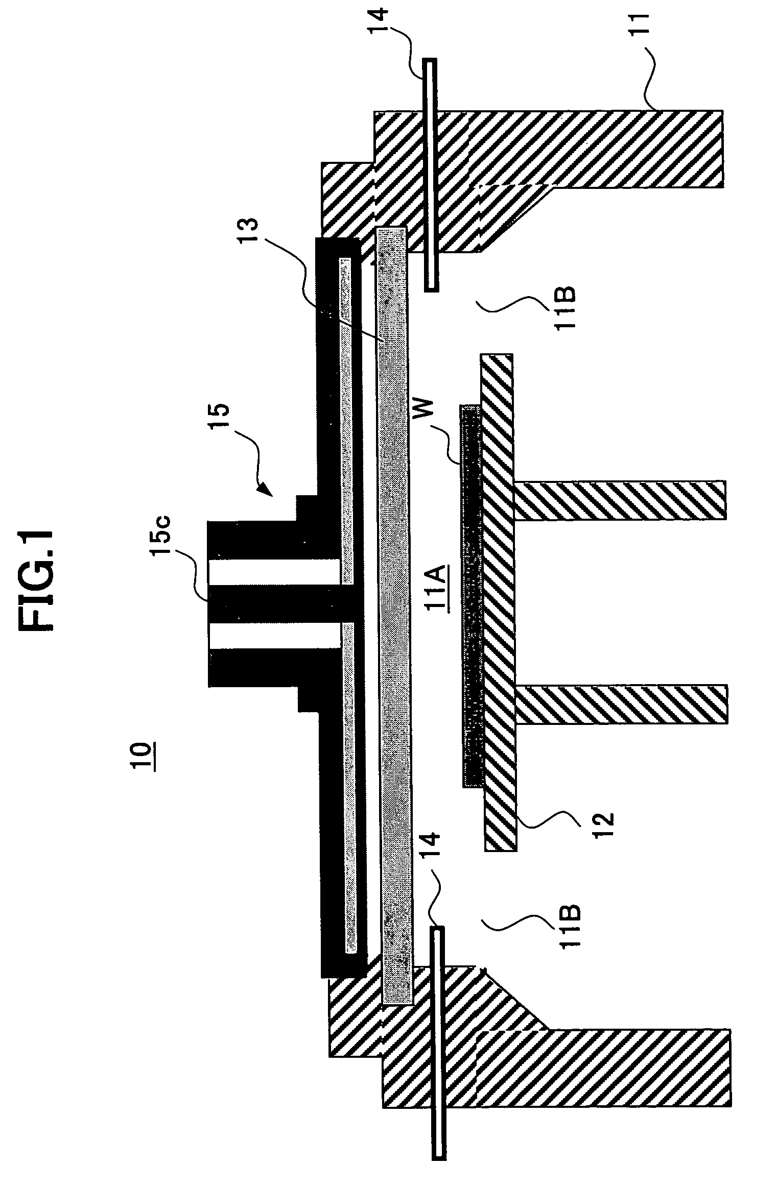
[0038]FIG. 1 shows the schematic construction of a plasma substrate processing apparatus 10 used with the present invention.
[0039]Referring to FIG. 1, the plasma substrate processing apparatus 10 includes a processing vessel 11 defining a processing space 11A evacuated through an evacuation port 11B, wherein the processing space 11A is provided with a stage 12 that supports a substrate W to be processed thereon. In the plasma processing apparatus 10 used with the present invention, the processing space 11A has a volume of 24 litters, for example.
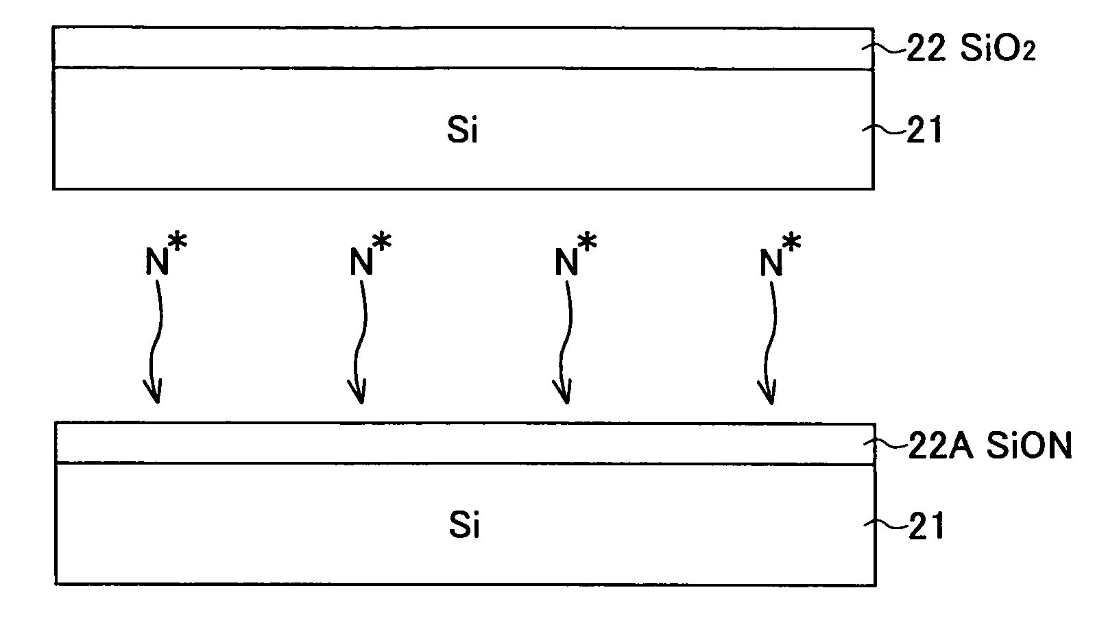
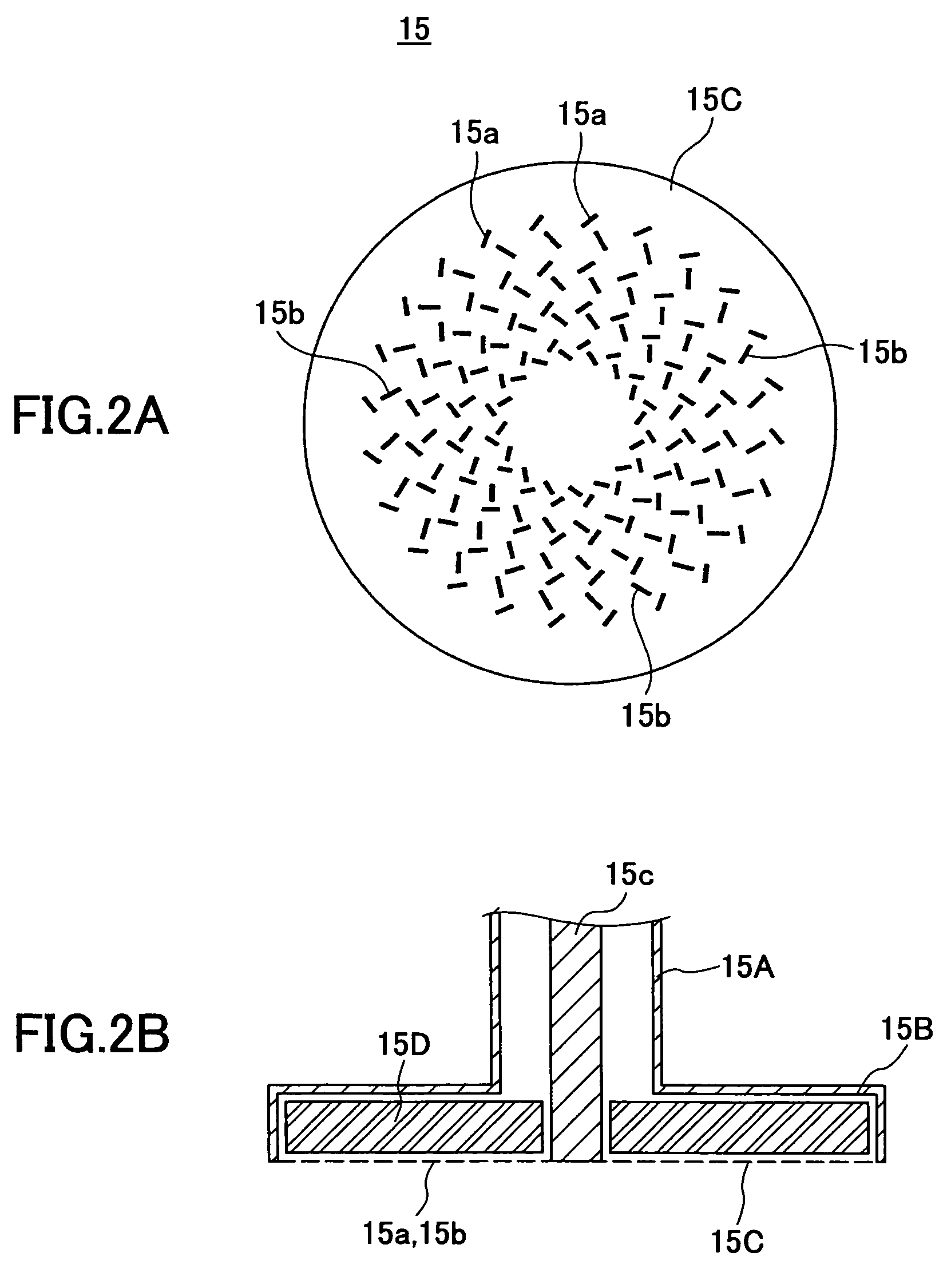
[0040]On the processing vessel 11, there is formed an opening in correspondence to the substrate W to be processed on the stage 12, and the opening is closed with a cover plate 13 of a low-loss dielectric such as quartz or alumina. Further, there are provided plural gas inlet ports 14 underneath the cover plate 13 in an axially symmetric relationship with regard to the substrate W to be processed.
[0041]Thereby, it should be...
second embodiment
[Second Embodiment]
[0089]FIG. 15 shows the construction of a CMOS device 40 according to a second embodiment of the present invention.
[0090]Referring to FIG. 15, the CMOS device 40 is formed on a silicon substrate 41 defined with device regions 41A and 41B by a device isolation structure 41C, wherein a p-type well is formed in the device region 41A while an n-type well is formed in the device region 41B.
[0091]On the device region 41A, there is formed a polysilicon gate electrode 43A via a gate insulation film 42A, and a polysilicon gate electrode 43B is formed on the device region 41B via a gate insulation film 42B. Further, n-type diffusion regions 41a and 41b are formed in the device region 41A at both sides of the gate electrode 43A. In the device region 41B, there are formed p-type diffusion regions 41c and 41d at both sides of the gate electrode 43B.
[0092]Further, sidewall insulation films 44A are formed at both sidewall surfaces of the gate electrode 43A, and sidewall insulati...
twelfth embodiment
[Twelfth Embodiment]
[0101]FIG. 19A shows the construction of an overall substrate processing system 100 that includes the substrate processing apparatus 10 of FIG. 1 and used for the nitridation processing of the oxide film of the present invention, while FIG. 19B show a computer used for controlling the substrate processing apparatus 10 of FIG. 1 in the system of FIG. 19A.
[0102]Referring to FIG. 19A, the system 100 includes an Ar gas source 101A and a nitrogen gas source 101B wherein the Ar gas source 101A supplies an Ar gas to the gas inlet port 14 of the substrate processing apparatus 10 via a mass flow controller 103A and via valves 104A and 105A and further via a valve 106, while the nitrogen gas source 101B supplies a nitrogen gas to the gas inlet port 14 via a mass flow controller 103N and via valves 104N and 105N and further via the valve 106 coupled to the gas inlet port 14 commonly to the gas supply path of the Ar gas and the gas supply path of the nitrogen gas.
[0103]Furth...
PUM
| Property | Measurement | Unit |
|---|---|---|
| temperature | aaaaa | aaaaa |
| time | aaaaa | aaaaa |
| time | aaaaa | aaaaa |
Abstract
Description
Claims
Application Information