High-accuracy pattern shape evaluating method and apparatus

a pattern shape and high-accuracy technology, applied in the direction of material analysis using wave/particle radiation, instruments, etc., can solve the problems of high method cost, high method cost, and damage to specimens, and achieve the effect of finer pattern shape evaluation, high accuracy roughness measurement, and easy short-term performan

Active Publication Date: 2007-06-12
HITACHI HIGH-TECH CORP
View PDF10 Cites 20 Cited by
  • Summary
  • Abstract
  • Description
  • Claims
  • Application Information

AI Technical Summary

Benefits of technology

[0027]As will be known from Ex. 3, an averaged profile is obtained by averaging S unaveraged profiles. Thus, it is expected that the power of noise on the profile is reduced greatly, or to approximately 1 / S, compared to that present when the profile was not averaged.
[0065]Once σA or A is calculated in any of the methods 5-1, 5-2 and 5-3, it can be used for analysis of patterns of the same design size created with the same materials in the same process. Among these three methods, method 5-1 that uses no fitting to obtain A or σA requires a shortest calculation time. Method 5-2 provides high accuracy and requires the operator to do a smallest quantity of work. Thus, method 5-2 is suitable for automation of the analysis work. Method 5-3 has a merit that as the number of measurement places increases, the measurement accuracy improves greatly.
[0067]In the above, the third method using Ex. 6 and the fourth and fifth methods using Ex. 7 have been illustrated. In any of these methods, only one fitting operation is required and a Fourier's conversion process can be omitted which imposes a burden on the calculation unit compared to the first and second methods that performs the averaging operations with the plurality of averaging parameter values, thereby obtaining edge roughness. Use of the third-fifth methods allows an error σe of roughness due to random noise to be quantified in a short time. In addition, a real roughness index value σ0 can be calculated and hence high-accuracy roughness of high throughput can be measured.
[0068]In the above, the principle of the means for obtaining roughness indexes has been described in each of the first-fifth methods. Since the first or second method includes the step of observing a spectrum visually, it has a merit that the user can immediately notice the occurrence of roughness having a peculiar period due to the influence of a mask or a peripheral pattern. Thus, this method is suitable for analysis of the characteristics of line-edge roughness of a circuit pattern in the semiconductor manufacturing process and / or a study of development of devices. The third method is suitable for analysis of an image in which a long area along the edge is observed at very fine scanning intervals because the ratio of σLOST (S) to the whole roughness is small. When a length along a line of the observation area is short or the scanning line intervals are large, a relative value of σLOST (S) to roughness to be measured is large. Thus, correction is required. Accordingly, in such a case the fourth method in which accurate measurement is possible by correction is suitable. In addition, when the number of scanning lines is small or the magnification of a (y-) direction along the edge is low, the fourth method is suitable because in such a case, Δy is large and a high frequency area on the spectrum is not observed, and hence the value of A cannot be obtained possibly in the fourth method in which the value of parameter A is fitted based only on the obtained data. If the fifth method in which σA S obtained beforehand from an image observed with higher magnification is used, A is determined with high accuracy and σ0 and σe can be calculated accurately.
[0072]The high-accuracy pattern shape evaluating method and apparatus according to the present invention has the function of quantifying the influence of random noise on line-edge roughness when a fine pattern is observed with the scanning microscope and calculating a value closer to real edge roughness by subtracting the quantified noise value from the measured value. In addition, these calculations can be performed based on a single sheet of observation image. In this calculation, the user need not perform a complicated operation such as parameter setting. Thus, high-accuracy roughness measurement can be performed easily in a short time even from an image of high noise, thereby allowing the finer pattern shape to be evaluated. This produces an advantageous effect that the examination time is reduced and deformation / damage of the pattern in observation is restricted, advantageously. Thus, in fine working, development of materials and processes and screening can be performed accurately with a low damage. Even in mass production process, high-accuracy examination is achieved, thereby improving productivity.
[0073]The influence of random noise quantified can be used as a noise index of the device. Using this result, it can be determined whether the observation conditions are good or not (for example, whether the microscope is in focus). By measuring and preserving this index over a long time, a long-time stability of the device performance can be evaluated, thereby improving productivity.

Problems solved by technology

Random noise occurring in the image acquirement will greatly influence this work.
First, damage to a specimen or changes in the dimensions of the specimen (due to pattern shrinkage, charging, adhesion of organic molecules, etc.) due to irradiation of the specimen with an electron beam can be a problem.
Second, there are demands for observation of only higher frequency components of the roughness.
In addition to these measurement parameters, the device performance and more particularly an extent of noise influence the measured values of the actual roughness indexes.
Occurrence of the bias is mainly due to noise.
The problem with the method disclosed in non-patent literature 2 is that first, the method is very time consuming.
Correction of the position deviation is time consuming and requires the operator's experience and data processing is complicated.
In addition, automation is difficult.
A second problem is to damage to the specimen.
As described above, the conventional method of calculating a bias component included in the line-edge or line width roughness needs two sets or more of image data and takes a long time for data processing.
Furthermore, the beam irradiation time for the specimen increases, thereby damaging the observation pattern possibly.

Method used


Image

  • High-accuracy pattern shape evaluating method and apparatus
  • High-accuracy pattern shape evaluating method and apparatus
  • High-accuracy pattern shape evaluating method and apparatus

Examples


embodiment 1

(Embodiment 1)

[0097]This embodiment illustrates application of the first method to a CD-SEM, which will be described next.

[0098]FIG. 18 schematically illustrates a hardware structure of the CD-SEM used in this embodiment. The CD-SEM mainly comprises housing 1801 of a scanning electron beam microscope that comprises an optoelectronic (or SEM) column and a specimen chamber, a control system 1811 for the microscope and information processor 1812. Information processor 1812 is connected to a data storage device 1813 that stores an obtained scanned electronic image and CAD data necessary for analyzing purposes. Data storage device 1813 can be provided within information processor 1812. Although not shown, information processor 1812 comprises an information input terminal that an operator of CD-SEM inputs information necessary for data processing to information processor 1812 and an image display means that displays a scanned electronic image acquired. A specified information input termin...

embodiment 2

(Embodiment 2)

[0116]The present embodiment relates to application of the second method to the CD-SEM, which will be described next. In order to describe the present embodiment, FIGS. 8, 9 and 10 will be used. The CD-SEM used in this embodiment has exactly the same hardware structure as the first embodiment. Thus, in the following, the description of Embodiment 1 concerning FIG. 18 will be used as requested.

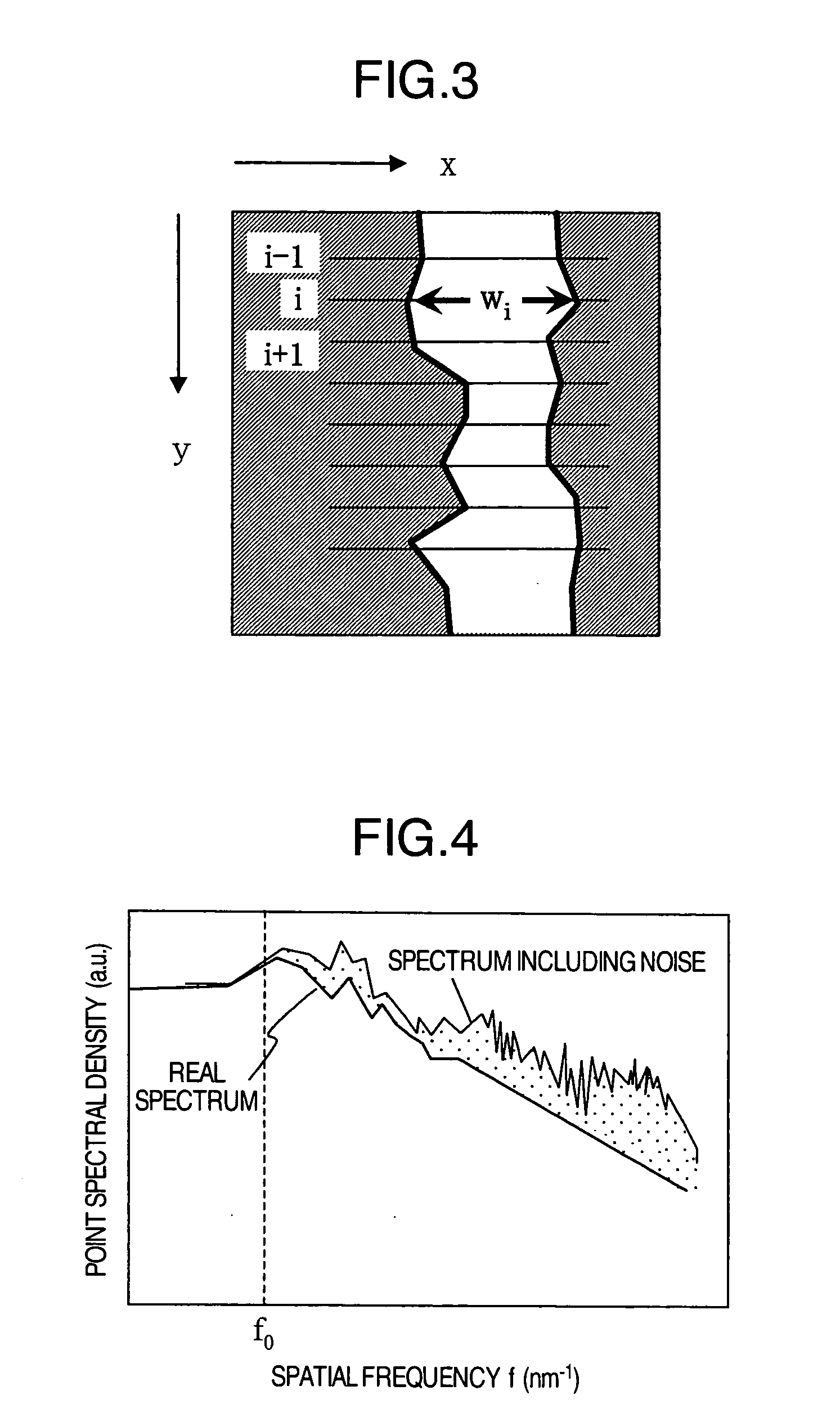
[0117]FIG. 8 schematically illustrates a SEM image of a pattern analyzed in the embodiment. FIG. 9 illustrates a display picture obtained by repeating the resetting of averaging parameter S until S=3. A process ranging from the setting of examination areas 803 and 804 of FIG. 8 to acquisition of the power spectrum of FIG. 9 is exactly the same as that of Embodiment 1.

[0118]As described in Embodiment 1, advent of the circumstances in which the power spectrum density of the high frequency area was directly proportional to 1 / f2 when S=3 was confirmed visually. On the other hand, howe...

embodiment 3

(Embodiment 3)

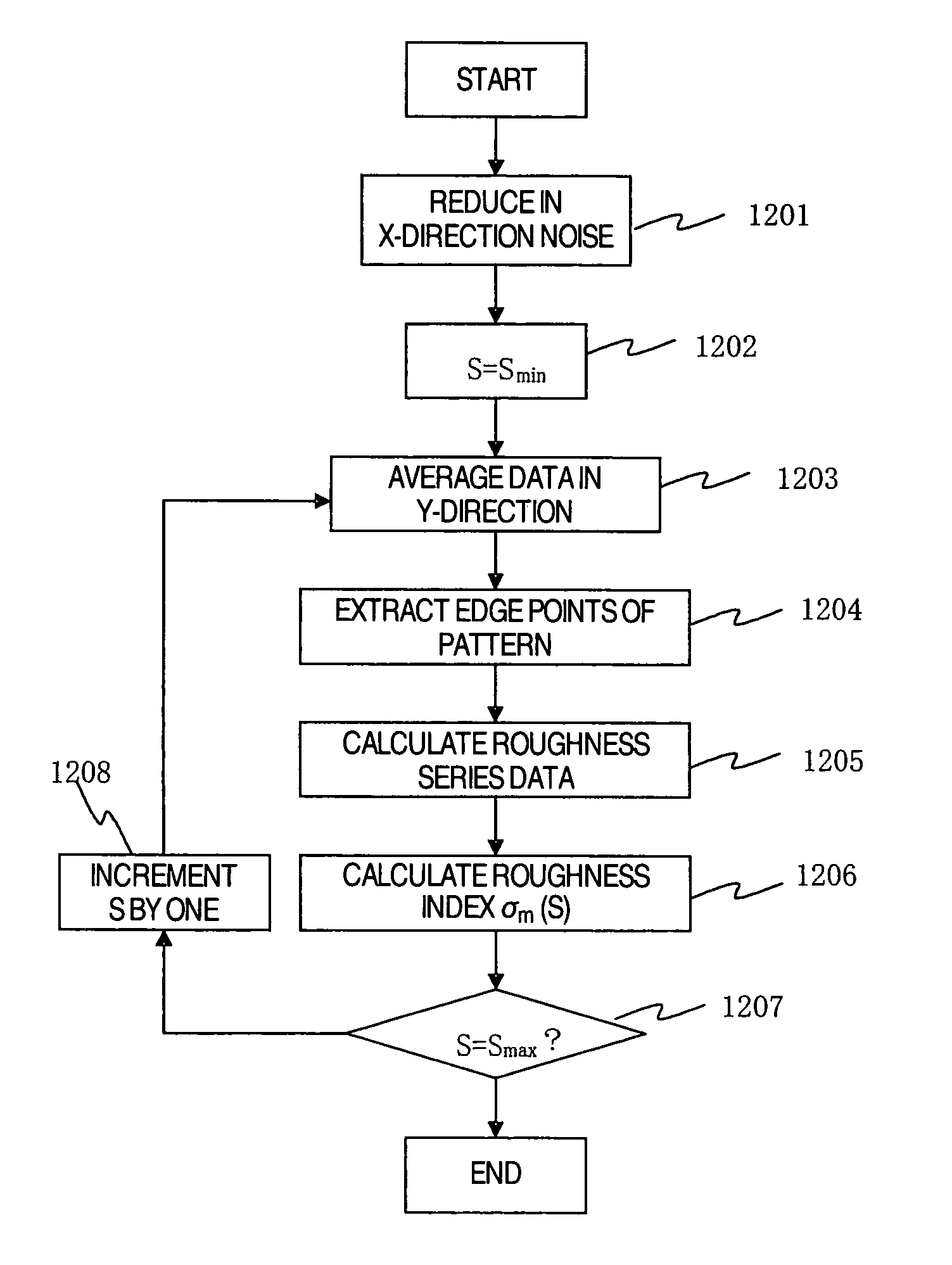
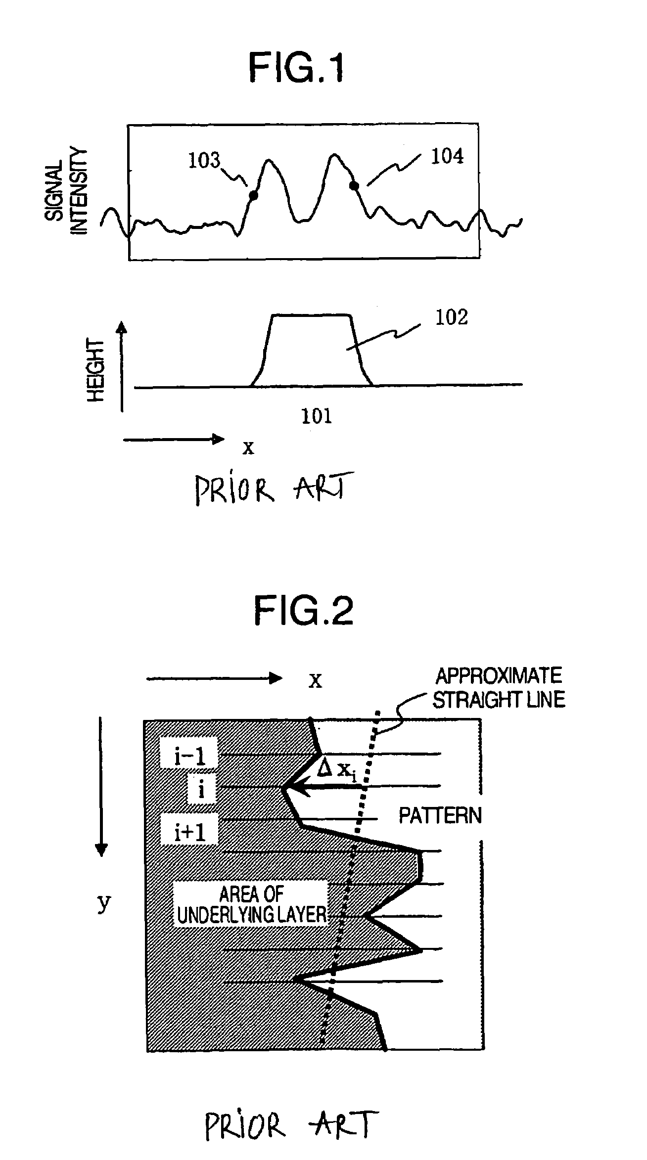
[0123]The present embodiment relates to application of the third method described in “Summary of the Invention” to the CD-SEM, which will be described next. The image data analysis method which will be described in the present embodiment comprises obtaining an index of roughness and an index of random noise occurring in the image without performing Fourier' transform from data used to calculate the roughness in Embodiment 1. In the description of the present embodiment, FIGS. 8, 11–14 will be used. FIG. 8 schematically illustrates a SEM image of a pattern analyzed in the present embodiment. FIG. 11 is a flowchart of a calculation process performed in the present embodiment. FIGS. 12 and 13 are flowcharts each representing a part of the process of FIG. 11. FIG. 14 shows roughness indexes obtained from the image and a graph of a fitting curve as a result of the analysis. The CD-SEM used in the present embodiment is exactly the same structure as used in Embodiment 1. Thus...


PUM

PropertyMeasurementUnit
lengthaaaaaaaaaa
lengthaaaaaaaaaa
roughnessaaaaaaaaaa

Abstract

A quantity (or dispersion value) of a distribution of edge position due to random noise is expected to be reduced statistically to 1 / N when N edge position data items are averaged. Using this property, the single page image is averaged in a vertical direction with various values of parameter S, and then the edge roughness index is calculated. The S-dependence of the edge roughness index is analyzed and a term of a dispersion value directly proportional to 1 / S is determined as being due to noise.

Description

INCORPORATION BY REFERENCE[0001]The present application claims priorities from Japanese applications JP2005-000029 filed on Jan. 4, 2005, JP2005-343047 filed on Nov. 29, 2005, the contents of which are hereby incorporated by reference into this application.BACKGROUND OF THE INVENTION[0002]The present invention relates to fine pattern examining methods and apparatus using detailed shape or size measurement based on non-destructive observation and image processing, with a scanning microscope and methods of evaluating the examining apparatus.[0003]In semiconductor and other industries, evaluation of fine roughness of randomly occurring pattern edges called edge roughness has been required as the pattern processing sizes become finer. Especially, in semiconductor process it has been known that a local fluctuation of a line width or line width roughness occurring from a (line) edge roughness or a line's right and left edge roughness of a gate or interconnect pattern will greatly influenc...

Claims


Application Information

Patent Timeline
Patent Type & Authority Patents(United States)
IPC IPC(8): G01B11/24G01N23/00
CPCG01N23/2251
Inventor YAMAGUCHI, ATSUKOFUKUDA, HIROSHIKOMURO, OSAMUKAWADA, HIROKI
Owner HITACHI HIGH-TECH CORP
Why Eureka
Try Eureka