Organic light-emitting device

a light-emitting device and organic technology, applied in the direction of discharge tube luminescnet screen, other domestic articles, natural mineral layered products, etc., can solve the problems of insufficient resolution and insufficient durability, and achieve the effects of high brightness, long life and high efficiency

Inactive Publication Date: 2007-06-19
CANON KK
View PDF33 Cites 137 Cited by
  • Summary
  • Abstract
  • Description
  • Claims
  • Application Information

AI Technical Summary

Benefits of technology

[0008]The present invention has been made to solve the above-mentioned problems of the conventional technologies, and an object of the present invention is to provide an organic light-emitting device that exhibits a light emission of extremely high efficiency, high brightness, and long lifetime.
[0009]Furthermore, another object of the present invention is to provide an organic light-emitting device that shows various emission wavelengths and various emission hues and that is extremely durable.
[0010]Moreover, another object of the present invention is to provide an organic light-emitting device that can not only be manufactured easily but also produced at a relatively low cost.

Problems solved by technology

Furthermore, there are still many problems in regard to durability such as change with elapse of time due to prolonged use and deterioration or the like, by moisture and the atmospheric gas containing oxygen.
Moreover, in view of application to a full-color display etc., blue, green, and red light emissions having higher color purities are needed, and this problem has not been solved sufficiently yet.

Method used


Image

  • Organic light-emitting device
  • Organic light-emitting device
  • Organic light-emitting device

Examples


example 1

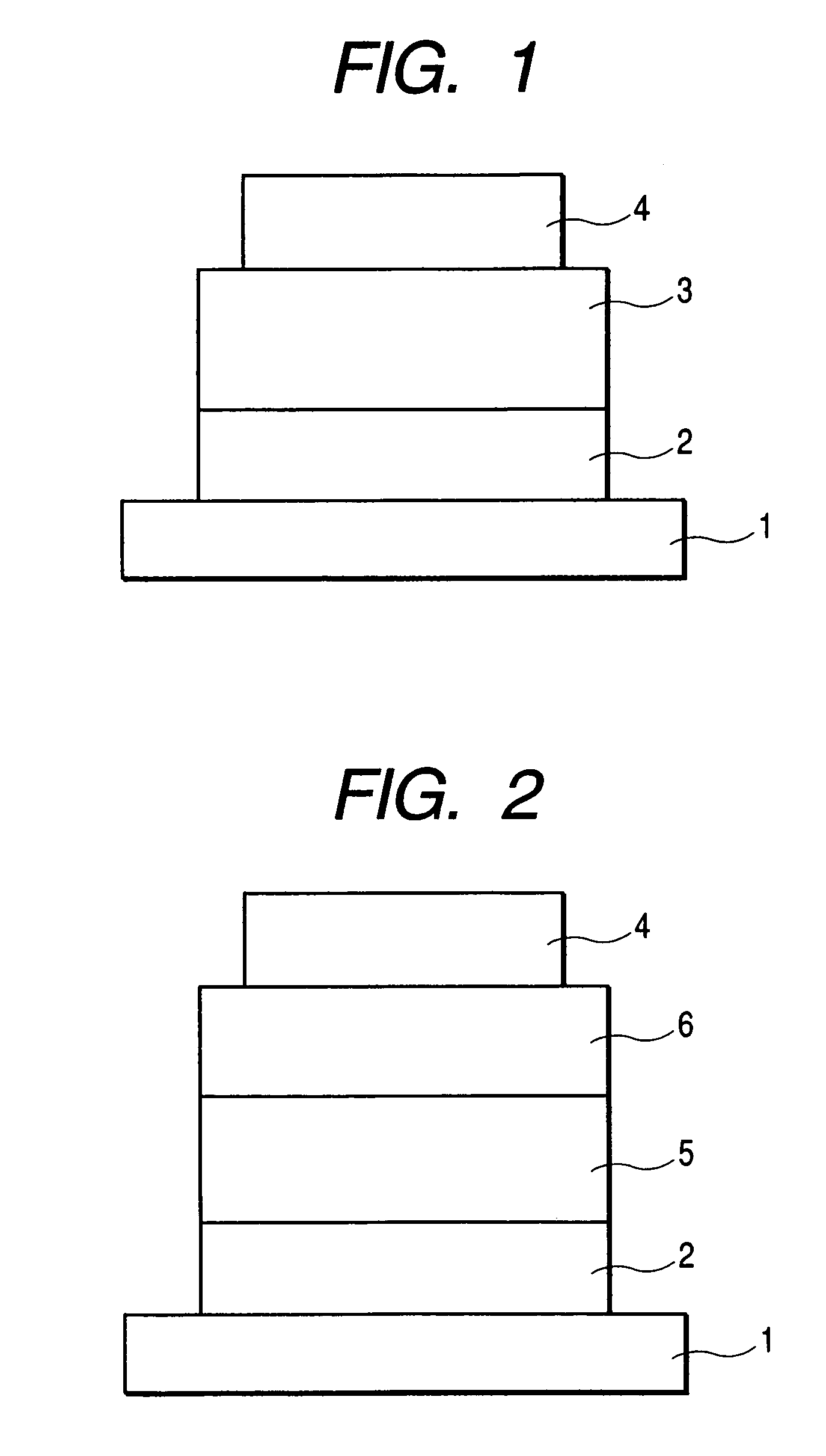
[0059]A device having a structure as shown in FIG. 1 was produced.

[0060]A transparent conductive supporting substrate was used which was produced by forming a film of indium-tin oxide (ITO) having a film thickness of 120 nm as an anode 2 on a glass substrate as a substrate 1 by means of sputtering method. This substrate was cleaned ultrasonically with acetone and isopropyl alcohol (IPA) in this order. After boiling cleaning with IPA, the substrate was dried. The substrate was further cleaned with UV / ozone and then was used as a transparent conducting supporting substrate.

[0061]A solution was prepared by dissolving 0.050 g of the compound shown as the above-exemplified compound No. 1 and 1.00 g of polyvinylcarbazole in 75 ml of tetrahydrofuran. Using this solution, an organic film layer (light-emitting layer 3) having a thickness of 120 nm was formed on a transparent conductive supporting substrate by means of spin coat method (2000 rpm).

[0062]Next, using a deposition material compos...

example 2

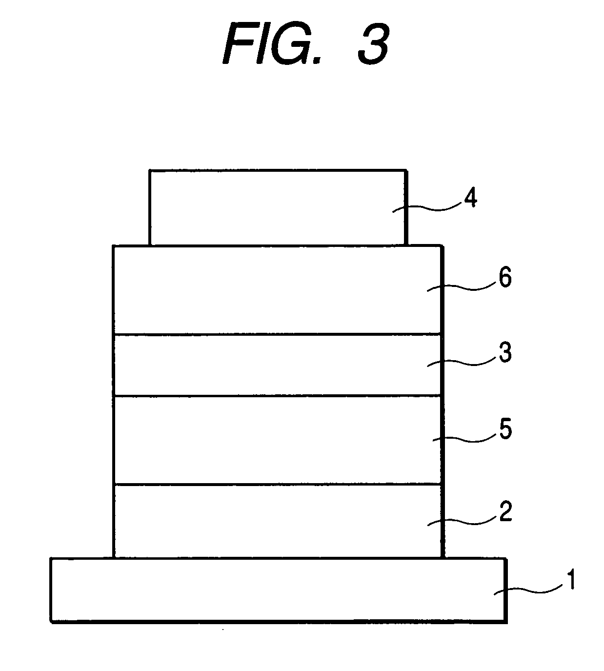
[0064]A device having a structure as shown in FIG. 2 was produced.

[0065]A hole-transporting layer 5 was formed by making α-NPD into a thin film having a thickness of 70 nm on a transparent conductive supporting substrate similar to that in Example 1 by means of vacuum vapor deposition method. Subsequently, an electron-transporting layer 6 was formed by making the exemplified compound No. 15 into a thin film having a thickness of 50 nm by means of vacuum vapor deposition method. The film formation was performed under the conditions where the degree of vacuum at the time of vapor deposition was 1.0×10⁻⁴ Pa, and the film-forming rate was 0.2 to 0.3 nm per second.

[0066]Next, a cathode 4 was formed on the above-mentioned organic layer in the same manner as in Example 1.

[0067]Using an ITO electrode as a positive electrode and an Al—Li electrode as a negative electrode, a direct current voltage of 8 V was applied to the device thus obtained, so that flow of an electric current having a cur...

example 3

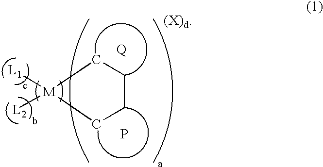
[0068]A device having a structure as shown in FIG. 3 was produced.

[0069]A hole-transporting layer 5 was formed by making TPD into a thin film having a thickness of 70 nm on a transparent conductive supporting substrate similar to that in Example 1 by means of vacuum vapor deposition method. A light-emitting layer 3 was formed by making the exemplified compound No. 1 into a thin film having a thickness of 40 nm by means of vacuum vapor deposition method. An electron-transporting layer 6 was formed by making aluminum trisquinolinol into a thin film having a thickness of 25 nm by means of vacuum vapor deposition method. The film formation was performed under the conditions where the degree of vacuum at the time of vapor deposition was 1.0×10⁻⁴ Pa, and the film-forming rate was 0.2 to 0.3 nm per second.

[0070]Next, a cathode 4 was formed on the above-mentioned organic layer in the same manner as in Example 1.

[0071]Using an ITO electrode as a positive electrode and an Al—Li electrode as a...


PUM

PropertyMeasurementUnit
thicknessaaaaaaaaaa
thicknessaaaaaaaaaa
thicknessaaaaaaaaaa

Abstract

An organic light-emitting device that exhibits a light emission of extremely high efficiency, high brightness, and long lifetime is provided. An organic light-emitting device includes a pair of electrodes including an anode and a cathode, and one or more layers containing an organic compound, the layers being sandwiched between the pair of the electrodes, characterized in that at least one layer of the layers containing an organic compound contains a compound represented by the following general formula (1)

Description

TECHNICAL FIELD[0001]The present invention relates to an organic light-emitting device, and more specifically to a device that emits light by applying an electric field to a thin film containing an organic compound.BACKGROUND ART[0002]Organic light-emitting devices are luminescent devices utilizing light that is emitted when excitons of fluorescent organic compounds move back to the ground state, the excitons being formed by sandwiching a thin film that contains the fluorescent compounds between an anode and a cathode and injecting electrons and holes (positive holes) from the respective electrodes.[0003]A study by Eastman Kodak Company in 1987 (Appl. Phys. Lett. 51, 913 (1987)) reports that a light emission of about 1000 cd / m2 was observed under an applied voltage of about 10 V. In the study, the device had a function-separated type bilayer structure and used ITO as the anode, a magnesium-silver alloy as the cathode, an aluminum quinolinol complex as an electron-transporting materi...

Claims


Application Information

Patent Timeline
Patent Type & Authority Patents(United States)
IPC IPC(8): H01L51/54C09K11/06H01L51/50H01L51/00H01L51/30
CPCC09K11/06H01L51/0084H01L51/0085H01L51/0087C09K2211/1003C09K2211/1007C09K2211/1011C09K2211/1029C09K2211/185C09K2211/187H01L51/0059H01L51/0081H01L51/0083H01L51/5012H01L2251/308Y10S428/917H10K85/631H10K85/331H10K85/324H10K85/341H10K85/342H10K85/346H10K50/11H10K2102/103
Inventor YAMADA, NAOKIUENO, KAZUNORI
Owner CANON KK
Why Eureka
Try Eureka