Reconfigurable switched-capacitor input circuit with digital-stimulus acceptability for analog tests

a switched-capacitor input circuit and digital stimulus technology, which is applied in the direction of digital-analog convertors, transmission systems, instruments, etc., can solve the problems of high testing cost of such products, long testing time, and disadvantageous fluctuation factors in both cost and time-to-market of products, so as to reduce test costs

Inactive Publication Date: 2007-06-26
NAT CHIAO TUNG UNIV
View PDF7 Cites 10 Cited by
  • Summary
  • Abstract
  • Description
  • Claims
  • Application Information

AI Technical Summary

Benefits of technology

[0009]The primary objective of the present invention is to provide a reconfigurable switched-capacitor input circuit with digital-stimulus acceptability for testing mixed-signal circuits, which carries out the tests of mixed-signal circuits via digital stimulus signals, would reduce the test cost.
[0010]A further objective of the present invention is to share critical circuit elements during testing thus offers high testing accuracy, high fault-coverage and the capability of performing at-speed tests owning to the shared critical circuit elements having the same loads in both test and normal operation modes.
[0011]A still further objective of the present invention is to provide a particular-designed reconfigurable circuit, which would apply for all kinds of the mixed-signal circuit architectures, for accelerating the design process and shortening the time-to-market.

Problems solved by technology

The testability and high testing cost of such products become a sever issue due to the diversity of the test characteristics of the embedded circuits.
And this issue is much more critical for the mixed-signal circuits since their tests traditionally have to rely on high-priced mixed-signal circuit testers like Aglient 94000.
Also, on account of most testers that do not support testing the analog circuit and digital circuit simultaneously, a longer testing time is required and makes disadvantageous fluctuation factors in both of the cost and time-to-market of the products.
Nevertheless, the testing accuracy depends on how accurate the ramp generator's output is and the generated ramp signal is not suitable for testing the circuits of either the Sigma-Delta modulator or the filter.
Consequently, higher cost for hardware and testing has to be endured.
In addition to the higher hardware cost, the built-in random-waveform generator would not carry out the at-speed tests.

Method used


Image

  • Reconfigurable switched-capacitor input circuit with digital-stimulus acceptability for analog tests
  • Reconfigurable switched-capacitor input circuit with digital-stimulus acceptability for analog tests
  • Reconfigurable switched-capacitor input circuit with digital-stimulus acceptability for analog tests

Examples


first embodiment

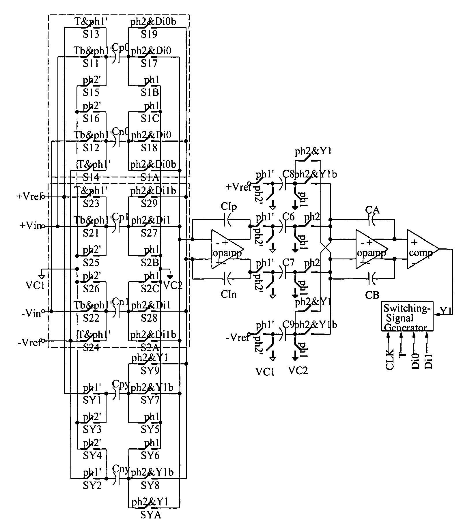
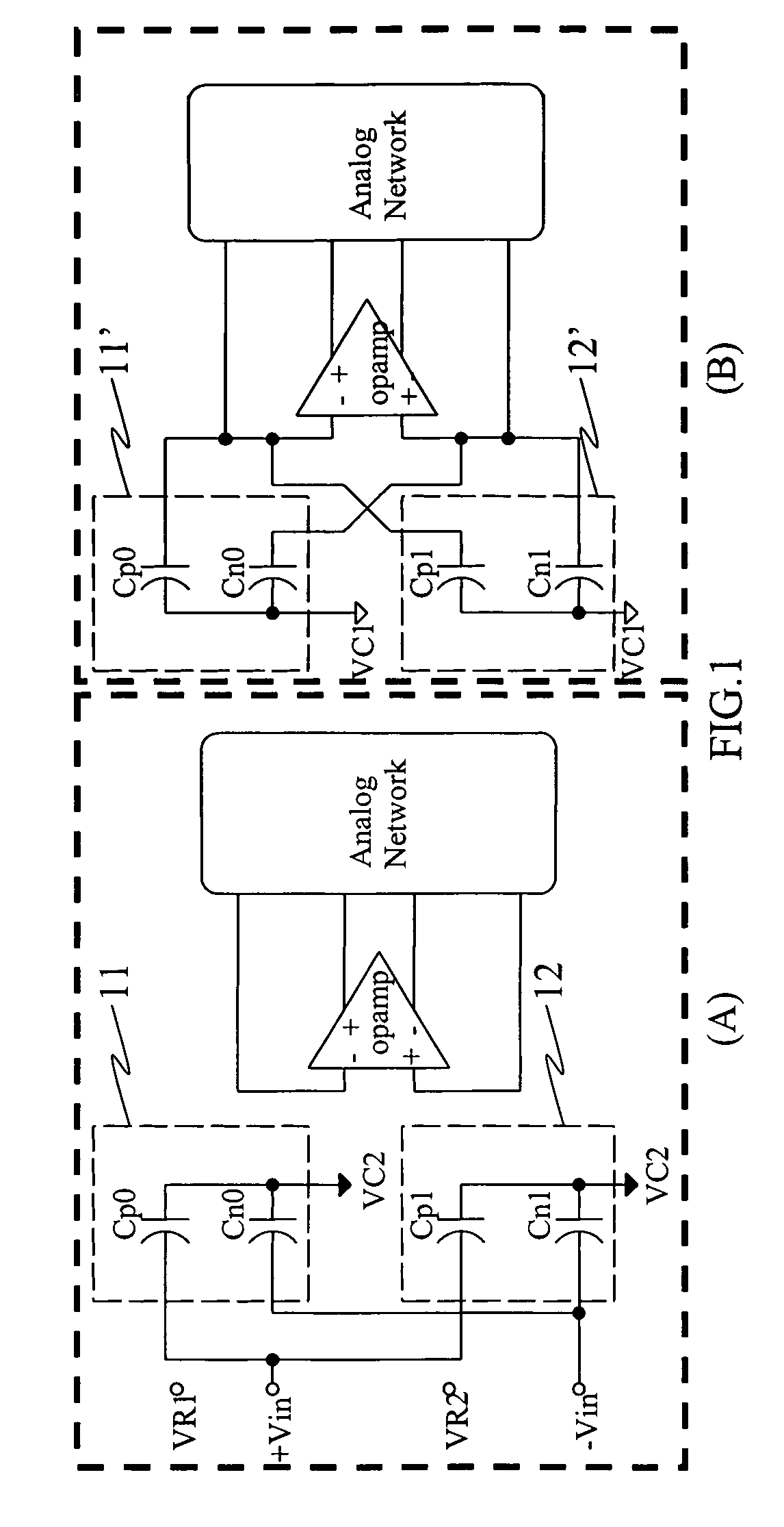
[0036]To better understand the operation of the reconfigurable switched-capacitor input circuit, the circuit connections in the two non-overlapped clock phases are described. FIG. 1 represents the operation of the reconfigurable switched-capacitor input circuit in the normal mode for the present invention that exerts at least two switched-capacitor sets. FIG. 1(A) shows the circuit connections in the first clock phase. The digital switching-signal generator generates the switching signals to control the analog-signal switches of the switched-capacitor sets 11 and 12 so that the bottom ends of the first capacitors Cp0 and Cp1 of the switched-capacitor sets connect to the analog input positive phase voltage signal +Vin and the bottom ends of the second capacitors Cn0 and Cn1 of the switched-capacitor sets connect to the analog input negative phase voltage signal −Vin. And all the top ends of the capacitors Cp0, Cn0, Cp1 and Cn1 connect to the direct current voltage source VC2. The cir...

second embodiment

[0040]Actually, the operation of the input circuit of the circuit under test in the normal mode is not limited by that revealed in FIG. 1. The second embodiment with regard to the reconfigurable switched-capacitor input circuit in the normal mode is introduced in FIG. 3, wherein FIG. 3(A) and FIG. 3(B) represent the circuit connections in the two non-overlapped clock phases respectively. The circuit connections of the input circuit in the first clock phase are provided in FIG. 3(A). The digital switching-signal generator generates the switching signals to connect the analog input positive phase voltage signal +Vin to the bottom ends of the first capacitors Cp0 and Cp1 of the switched-capacitor sets 31 and 32 and, in the meantime, to connect the analog input negative phase voltage signal −Vin to the bottom ends of the second capacitors Cn0 and Cn1 of the switched-capacitor sets 31 and 32. The top ends of the first capacitors of the switched-capacitor sets are connected to the negativ...

third embodiment

[0042]Additionally, the test mode operation of this invention whose normal mode operation is described in FIG. 1 is unfolded in FIG. 4. Similar to the disclosure in FIG. 2, the circuit connections in the two non-overlapped clock phases in the test mode are shown in FIG. 4(A) and FIG. 4(B) respectively. In the first clock phase, the digital switching-signal generator generates the switching signals to control the analog-signal switches of the switched-capacitor sets 41 and 42 to make the top ends of the capacitors Cp0, Cn0, Cp1 and Cn1 inside the switched-capacitor sets 41 and 42 connecting to the direct current voltage source VC2 as illustrated in FIG. 4(A). At the same time, the bottom ends of the first capacitors Cp0 and Cp1 and the second capacitors Cn0 and Cn1 inside the switched-capacitor sets 41 and 42 are connected to the direct current voltage source VR1 and the direct current voltage source VR2 respectively. One part of what illustrated in FIG. 4(B) is that all the bottom e...


PUM


Abstract

A reconfigurable switched-capacitor input circuit with digital-stimulus acceptability for analog tests disclosed in the present invention provides the digital input interfaces, which are comprised of capacitors, analog switches and digital circuits, for the usage of testing the mixed-signal circuits. The present invention provides a low-priced testing platform to accomplish the testing of circuits and to solve the problems of high-cost mixed mode tester and of utmost restrictions against the surrounding condition. Therefore, the present invention improves the testability, reduces the test cost, shorten the processes of designation and efficiently seize on the time-to-market.

Description

BACKGROUND OF THE INVENTION[0001]1. Field of Invention[0002]The invention is related to a reconfigurable switched-capacitor input circuit, and more particularly, to a reconfigurable switched-capacitor input circuit with digital-stimulus acceptability for testing mixed-signal circuits.[0003]2. Description of the Related Art[0004]At all electronics and electrical manufacturers focus on the family amusement market of meanwhile, makes the audio chip market growing up significantly. Hence, the test for a mixed-signal component that is comprised of the switched-capacitor circuits, such as the Sigma-Delta modulators, becomes more and more important. The evolution of the integrated circuit manufacture technology allows integrating diverse components such as digital, analog, and memory circuits on the same chip. The testability and high testing cost of such products become a sever issue due to the diversity of the test characteristics of the embedded circuits. And this issue is much more cri...

Claims


Application Information

Patent Timeline
Patent Type & Authority Patents(United States)
IPC IPC(8): H03M1/66
CPCH03M3/378H03M3/458
Inventor HONG, HAO-CHIAO
Owner NAT CHIAO TUNG UNIV
Why Eureka
Try Eureka