Growth of textured gallium nitride thin films on polycrystalline substrates

a gallium nitride and thin film technology, applied in the direction of crystal growth process, polycrystalline material growth, chemically reactive gas growth process, etc., can solve the problems of high density of dislocation and stress in the film

Inactive Publication Date: 2007-07-03
UNIV OF LOUISVILLE RES FOUND INC
View PDF1 Cites 5 Cited by
  • Summary
  • Abstract
  • Description
  • Claims
  • Application Information

AI Technical Summary

Benefits of technology

[0008]A synthesis route to grow textured thin film of gallium nitride on amorphous quartz substrates, on single crystalline substrates such as c-sapphire, and on polycrystalline substrates such as pyrolytic boron nitride (PBN), alumina and quartz using the dissolution of atomic nitrogen rather than molec

Problems solved by technology

The lattice mismatch and different thermal expansion coefficients between Ga

Method used


Image

  • Growth of textured gallium nitride thin films on polycrystalline substrates
  • Growth of textured gallium nitride thin films on polycrystalline substrates
  • Growth of textured gallium nitride thin films on polycrystalline substrates

Examples


Embodiment Construction

[0046]This method uses low pressure bulk synthesis to get large area, self oriented, high quality thin film GaN which avoids epitaxy using either tin molten gallium film as a buffer layer or directly growing on an amorphous substrate.

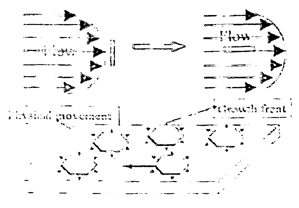
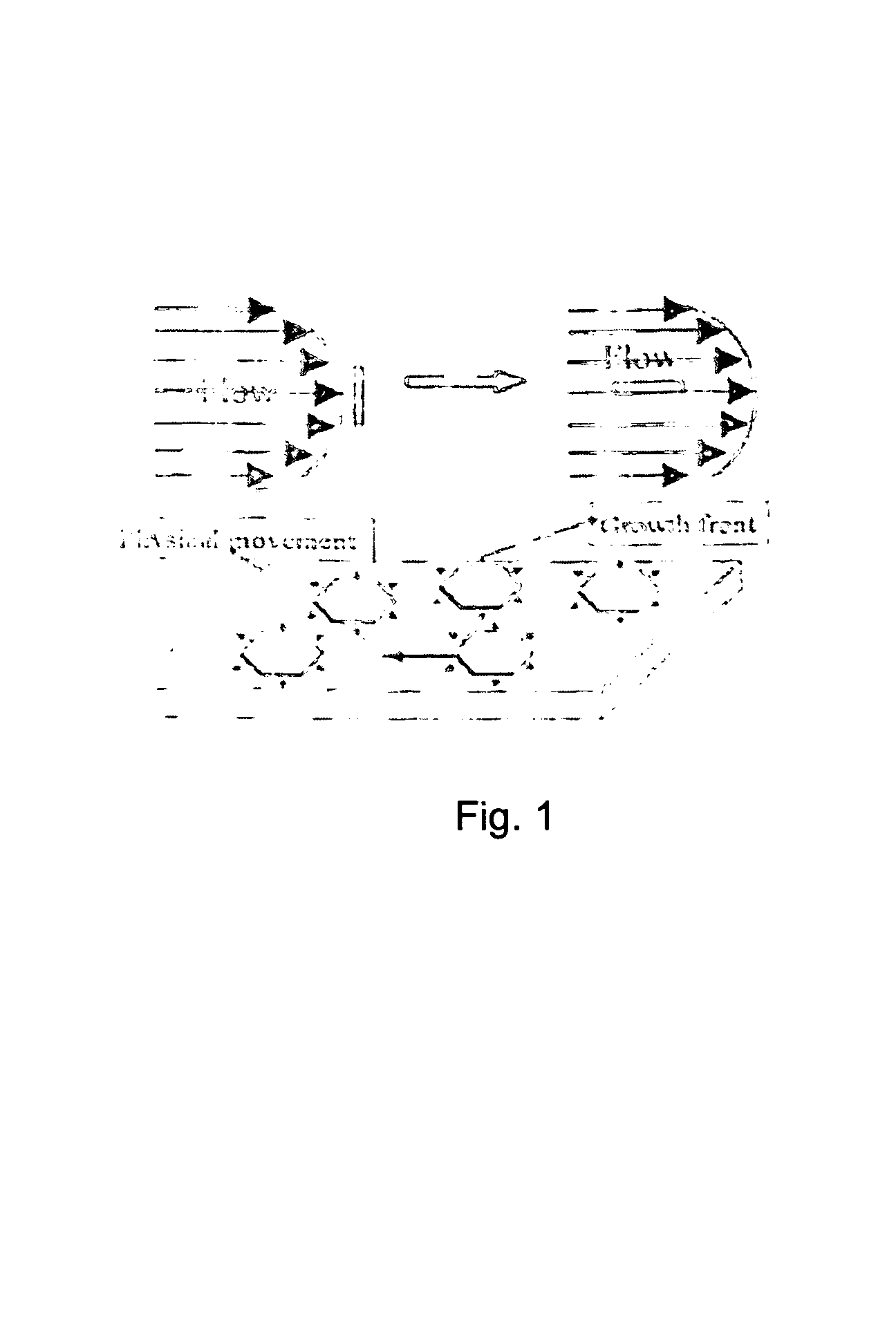
[0047]Thin films of liquid gallium are spread onto a single crystalline, polycrystalline or amorphous substrate, and then nitrided in an ECR-MW nitrogen plasma environment. Since nitrogen containing gallium melts wet solid surfaces very well, the flow of nitrided gallium melts will allow growing CaN platelets crystals to self-orient with respect to each other. The self-alignment of CaN crystlas occurs parallel to the flow direction and the growing platelets join together by self-assembly process (FIG. 1). As mentioned above, this process is essentially independent of substrates.

Self Oriented GaN growth on polycrystalline substrates

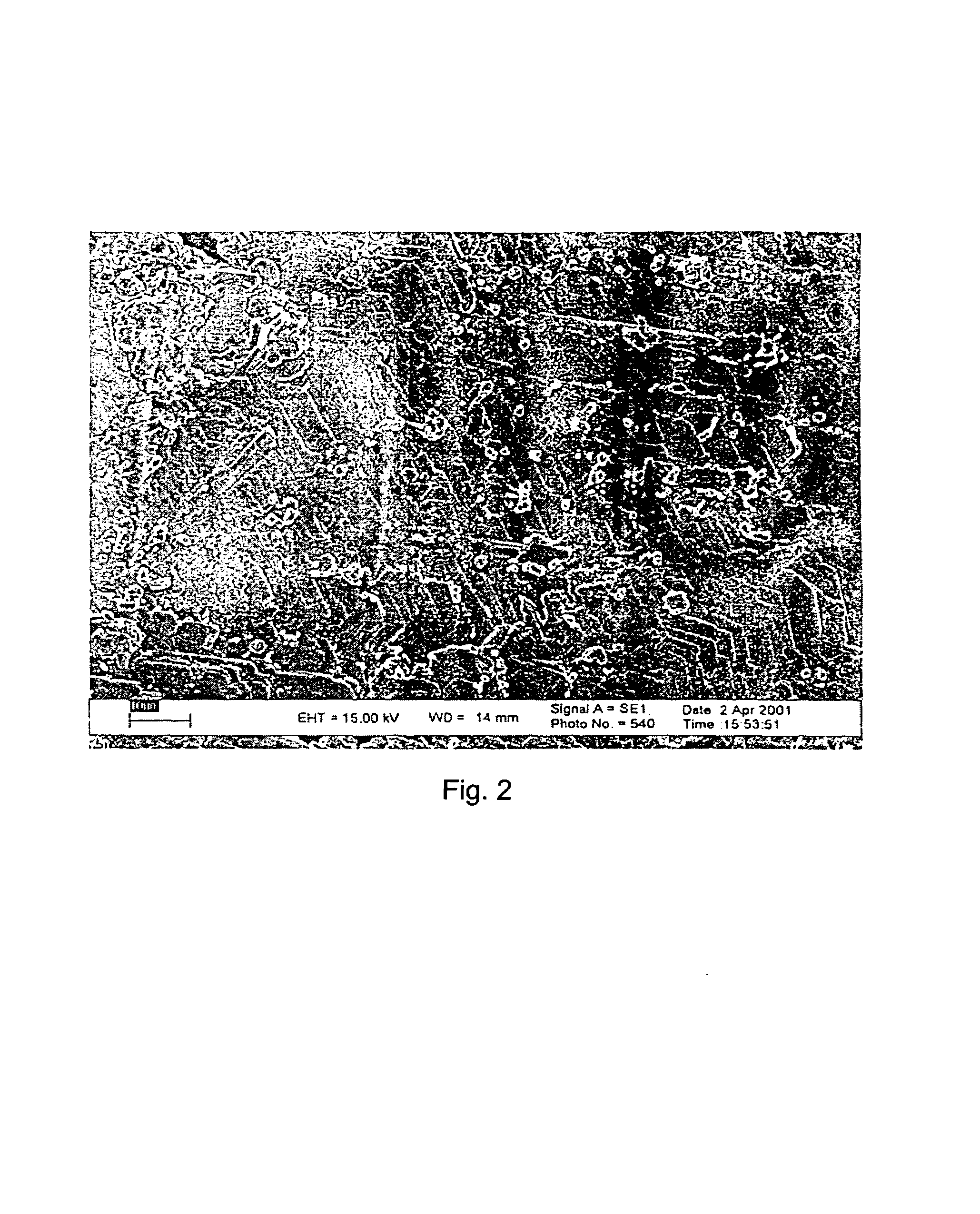
[0048]A novel synthesis route is provided to grow textured thin film of gallium nitride (GaN) on polycrystalline substrates ...


PUM


Abstract

A synthesis route to grow textured thin film of gallium nitride on amorphous quartz substrates and on single crystalline substrates such as c-sapphire and polycrystalline substrates such as pyrolytic boron nitride (PBN), alumina and quartz using the dissolution of atomic nitrogen rather than molecular nitrogen to allow for growth at subatmospheric pressure.

Description

[0001]This application claims priority form U.S. Provisional Application Ser. No. 60 / 376,492 filed on Apr. 30, 2002.[0002]This application is part of a government project. The research leading to this invention was supported by a Grant Number CTS9876251 from the U.S. Air Force. The United States Government retains certain rights in this invention.BACKGROUND OF THE INVENTION[0003]1. Field of the Invention[0004]The invention relates to the field of providing a synthesis technique to grow a film or small wire of gallium nitride on amorphous quartz substrates and on single crystalline substrates such as c-sapphire and polycrystalline substrates.[0005]2. Description of the Prior Art[0006]Gallium nitride (GaN) is a direct, wide band gap semiconductor that finds applications in light emitting diodes (LED), laser diodes (LD), high temperature / power field effect transistors (FET) and UV optical devices. Since both GaN substrates and lattice matched substrates are unavailable, hetero-epitaxy ...

Claims


Application Information

Patent Timeline
IPC IPC(8): C30B25/12
CPCC30B19/04C30B29/406C30B9/06
Inventor SUNKARA, MAHENDRA KUMARCHANDRASEKARAN, HARILI, HONGWEI
Owner UNIV OF LOUISVILLE RES FOUND INC
Why Eureka
Try Eureka