Thin wafer detectors with improved radiation damage and crosstalk characteristics

a technology of crosstalk and detectors, which is applied in the direction of photoelectric discharge tubes, instruments, radiation controlled devices, etc., can solve the problems of adversely affecting the performance of detectors, detectors showing an increased reverse-bias current, and increased forward voltage drop, so as to reduce radiation damage susceptibility, reduce crosstalk effects, and reduce dark current

Inactive Publication Date: 2007-07-10
OSI OPTOELECTRONICS
View PDF39 Cites 59 Cited by
  • Summary
  • Abstract
  • Description
  • Claims
  • Application Information

AI Technical Summary

Benefits of technology

[0010]The present invention is directed toward a detector structure, detector arrays, and a method of detecting incident radiation. The present invention comprises several embodiments that provide for reduced radiation damage susceptibility, decreased affects of crosstalk, reduced dark current (current leakage) and increased flexibility in application. In one embodiment, the present invention comprises a back side illuminated photodiode array with a back side etching that minimizes the active area layer, thereby decreasing the affects of crosstalk. The back side etch

Problems solved by technology

One problem with detection devices is that they are susceptible to various radiation damage mechanisms, such as displacement damage resulting in total dose effects and ionization damage resulting in bulk effects.
Both these mechanisms adversely affect the performance of detectors, transistors and integrated circuits.
Over time, detectors show an increased reverse-bias current and increased forward voltage drop due to radiation damage.
Further, a change in doping level, due to radiation damage, adversely affects the width of the depletion region, i.e. the voltage required for full depletion and a decrease in carrier lifetime results in signal loss as carriers recombine while traversing the depletion region.
Another disadvantage with conventional det

Method used


Image

  • Thin wafer detectors with improved radiation damage and crosstalk characteristics
  • Thin wafer detectors with improved radiation damage and crosstalk characteristics
  • Thin wafer detectors with improved radiation damage and crosstalk characteristics

Examples


Embodiment Construction

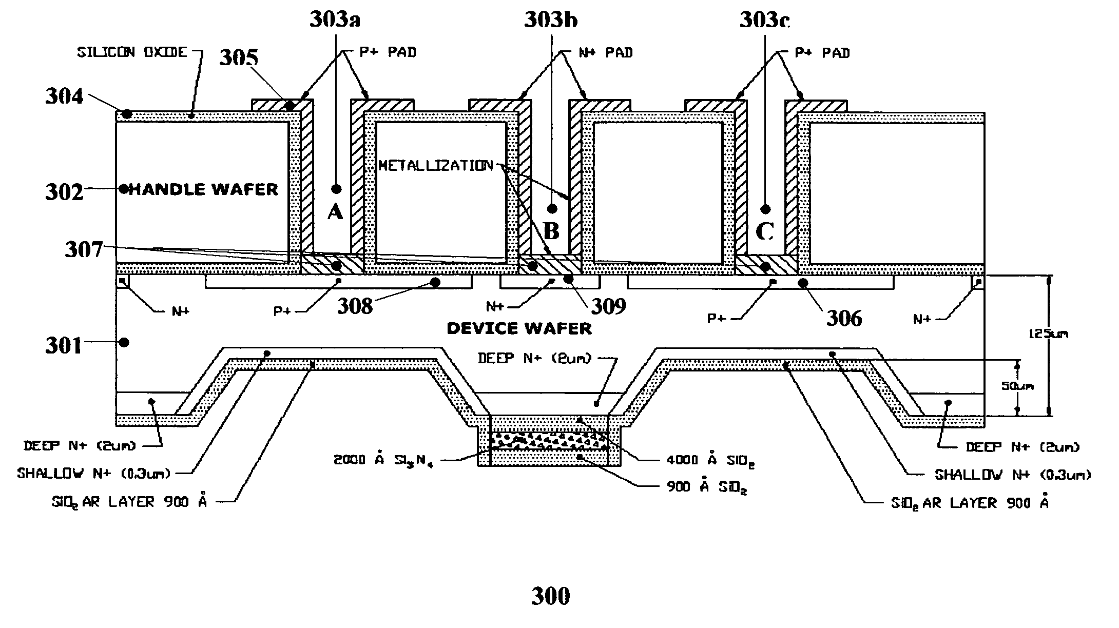
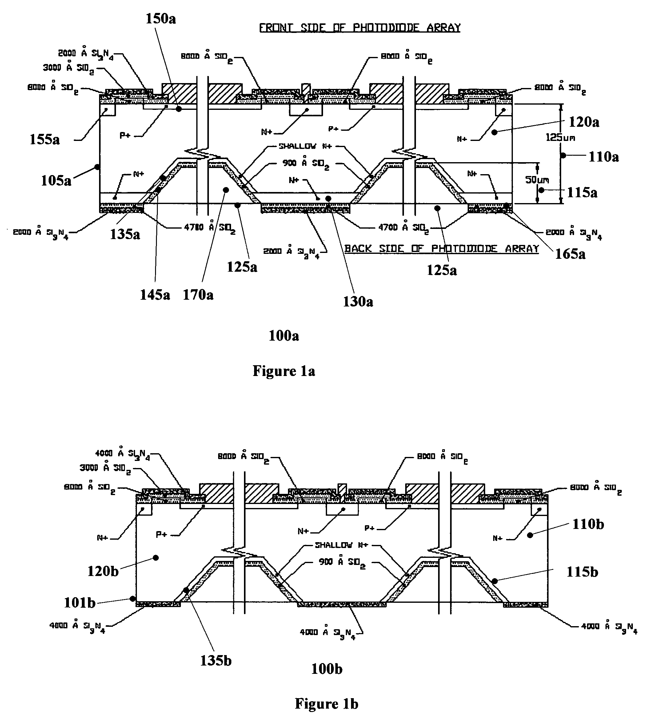
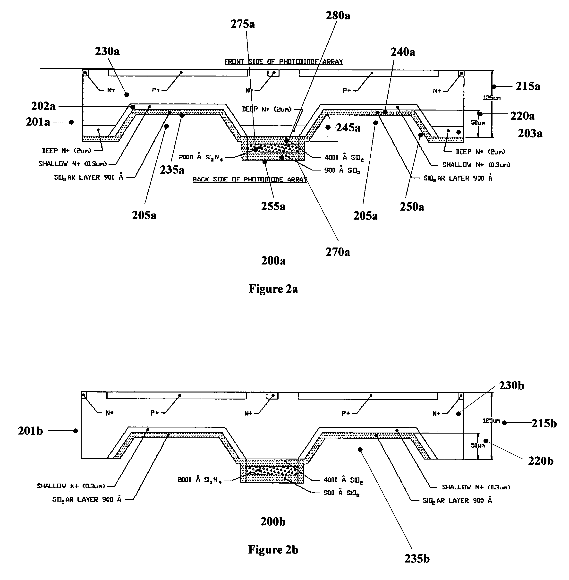
[0028]This application hereby incorporates by reference co-pending application, entitled “FRONT ILLUMINATED BACK SIDE CONTACT THIN WAFER DETECTORS”, which also relies on, for priority, U.S. Provisional Application 60 / 468,181, having a priority date of May 5, 2003, entitled “DETECTORS WITH IMPROVED RADIATION DAMAGE AND CROSSTALK CHARACTERISTICS”. The invention described therein comprises a plurality of front side illuminated photodiodes, optionally organized in the form of an array, with both the anode and cathode contact pads on the back side. The front side illuminated, back side contact (FSL-BSC) photodiodes have superior performance characteristics, including less radiation damage, less crosstalk using a suction diode, and reliance on reasonably thin wafers. The invention, as described therein, is a photodiode array having a substrate with at least a front side and a back side; a plurality of photodiodes integrally formed in the substrate forming the array wherein each photodiode...


PUM


Abstract

The present invention provides for reduced radiation damage susceptibility, decreased affects of crosstalk, and increased flexibility in application. In one embodiment, the present invention includes a back side illuminated photodiode array with a back side etching that minimizes the active area layer, thereby decreasing the affects of crosstalk. The back side etching is preferably, but by no way of limitation, in the form of “U” or “V” shaped grooves. The back side illuminated with back side etching (BSL-BE) photodiodes are implemented in an array and have superior performance characteristics, including less radiation damage due to a thinner active area, and less crosstalk due to shorter distances for minority carriers to diffuse to the PN junction.

Description

CROSS REFERENCE TO RELATED APPLICATIONS[0001]This invention relies on, for priority, U.S. Provisional Application 60 / 468,181, having a priority date of May 5, 2003, entitled “DETECTORS WITH IMPROVED RADIATION DAMAGE AND CROSSTALK CHARACTERISTICS”.FIELD OF THE INVENTION[0002]The present invention pertains generally to the field of radiation detectors, and in particular, relates to radiation detectors manufactured with thinner wafers, thereby yielding reduced crosstalk between detecting regions and decreased susceptibility to radiation damage, having front surface contacts.BACKGROUND OF THE INVENTION[0003]Arrays of photosensitive diodes are used in an assortment of applications including, but not limited to, radiation detection, optical position encoding, and low light-level imaging, such as night photography, nuclear medical imaging, photon medical imaging, multi-slice computer tomography (CT) imaging, and ballistic photon detection etc. Typically, photodiode arrays may be formed as ...

Claims


Application Information

Patent Timeline
IPC IPC(8): H01L31/00H01J40/14H01L21/00H01L27/146
CPCH01L27/1464H01L27/14643
Inventor BUI, PETER STEVENTANEJA, NARAYAN DASS
Owner OSI OPTOELECTRONICS
Why Eureka
Try Eureka