
Thin-film large-area coherent light source, filter and amplifier apparatus and method

a large-area coherent, thin-film technology, applied in the field of large-area, thin-film laser sources, can solve the problems of light sources, leds do not provide the performance needed for certain applications, and manufacture of vcsels requires sophisticated and expensive microfabrication, and achieves excellent efficient wide-area coherent lasing medium, facilitate heat extraction and high-power operation, and stable coherence area of the resulting lasing beam.

Inactive Publication Date: 2007-07-10
CHIRAL PHOTONICS
View PDF1 Cites 24 Cited by
  • Summary
  • Abstract
  • Description
  • Claims
  • Application Information

AI Technical Summary

Benefits of technology

[0018]In another embodiment of the present invention, the inventive apparatus is utilized as a passive spatial filter without requiring an active excitable material or a power source. A light source emits light at the frequency F which encompasses a range of wave vectors. The feedback structure only permits light of the particular frequency F that is within a narrow range in angle about the normal vector to the surface of the structure. Thus, the inventive apparatus can be advantageously utilized as a passive spatial filter for filtering out oblique components of light of the predefined frequency F and thereby expanding the output beam.
[0021]In an alternate lasing apparatus embodiment of the present invention, the LDP light source is utilized as an optical pump. The LDP light source emits light at a distributed substantially normal vector into a feedback structure. The feedback structure is preferably doped with optically excitable materials. Variable gain is applied by adjusting one or more emitters of the LDP light source. Preferably, the variable gain is applied above a lasing threshold such that lasing light is produced. Because the diffuser panel only emits light at an substantially normal vector, the structure provides an excellent efficient wide-area coherent lasing medium. In accordance with the present invention even if gain is varied above the lasing threshold the coherence area of the resulting lasing beam remains stable.
[0022]The inventive apparatus and method advantageously overcome the drawbacks of previously known edge-emitting lasers and VCSELs by providing wide-area coherent lasing with transverse dimensions that can be much greater than the thickness of the feedback structure utilized in the inventive apparatus. This is possible at the laser wavelength because only a single narrow mode of radiation exists over a wide angular range centered at the normal direction. The spread of optical coherence is diffusion-like, resulting in a beam width, which is proportional to the square root of the photon dwell time. The use of the inventive large-area, thin-film laser facilitates heat extraction and high power operation. Thus, the properties of the inventive apparatus may enable lightweight optical sources for free-space communication, coherent backlighting for 3-D holographic and projection displays, and therapeutic irradiation of large areas of skin among other applications.

Problems solved by technology

However, previously known semiconductor lasers have a number of disadvantages.
Other types of light sources, such as LEDs do not provide the performance needed for certain applications.
The manufacture of VCSELs requires sophisticated and expensive microfabrication.
However, this approach makes the fabrication more expensive and difficult.
While VCSELs can be manufactured in two-dimensional arrays, there has been great difficulty in achieving uniform structure over large areas and in producing large area arrays.
The materials typically used for VCSELs do not have the desired low absorption and high index contrast over a broad frequency range.
In particular, it is difficult to achieve high reflectivity in the communication band around 1.5 microns.
In addition, VCSELs cannot be tuned in frequency since their periods cannot be changed.
The density of photon modes is not changed appreciably by use of low index contrast multilayer Bragg reflector and the gain cannot be improved in a VCSELs system as compared to that in an ordinary laser cavity.
It should also be noted that VCSELs inherently do not allow for large area coherence because their length is greater than the diameter, and because they are comprised of alternating layers with low index contrast.

Method used


Image

  • Thin-film large-area coherent light source, filter and amplifier apparatus and method
  • Thin-film large-area coherent light source, filter and amplifier apparatus and method
  • Thin-film large-area coherent light source, filter and amplifier apparatus and method

Examples


first embodiment

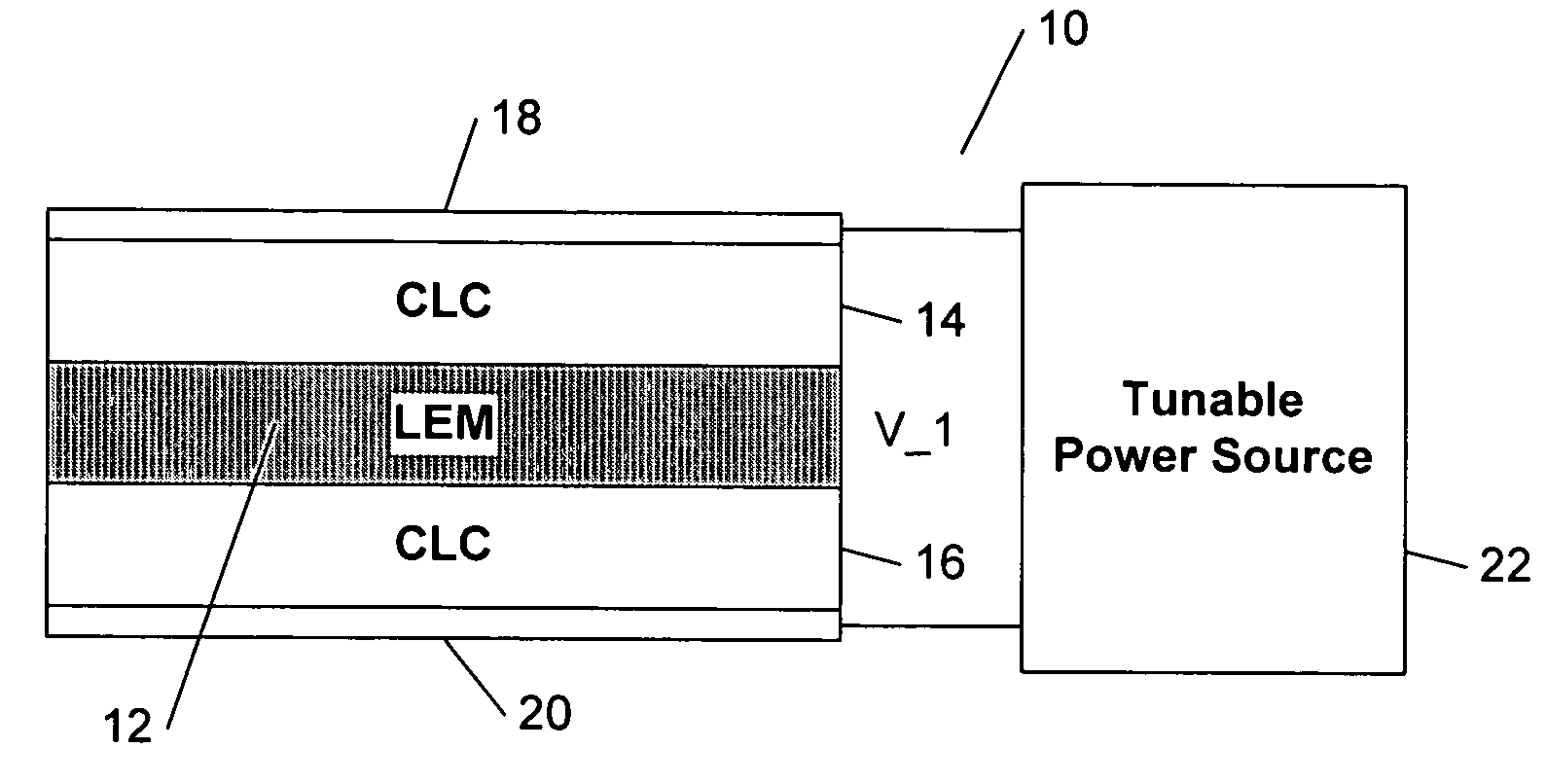
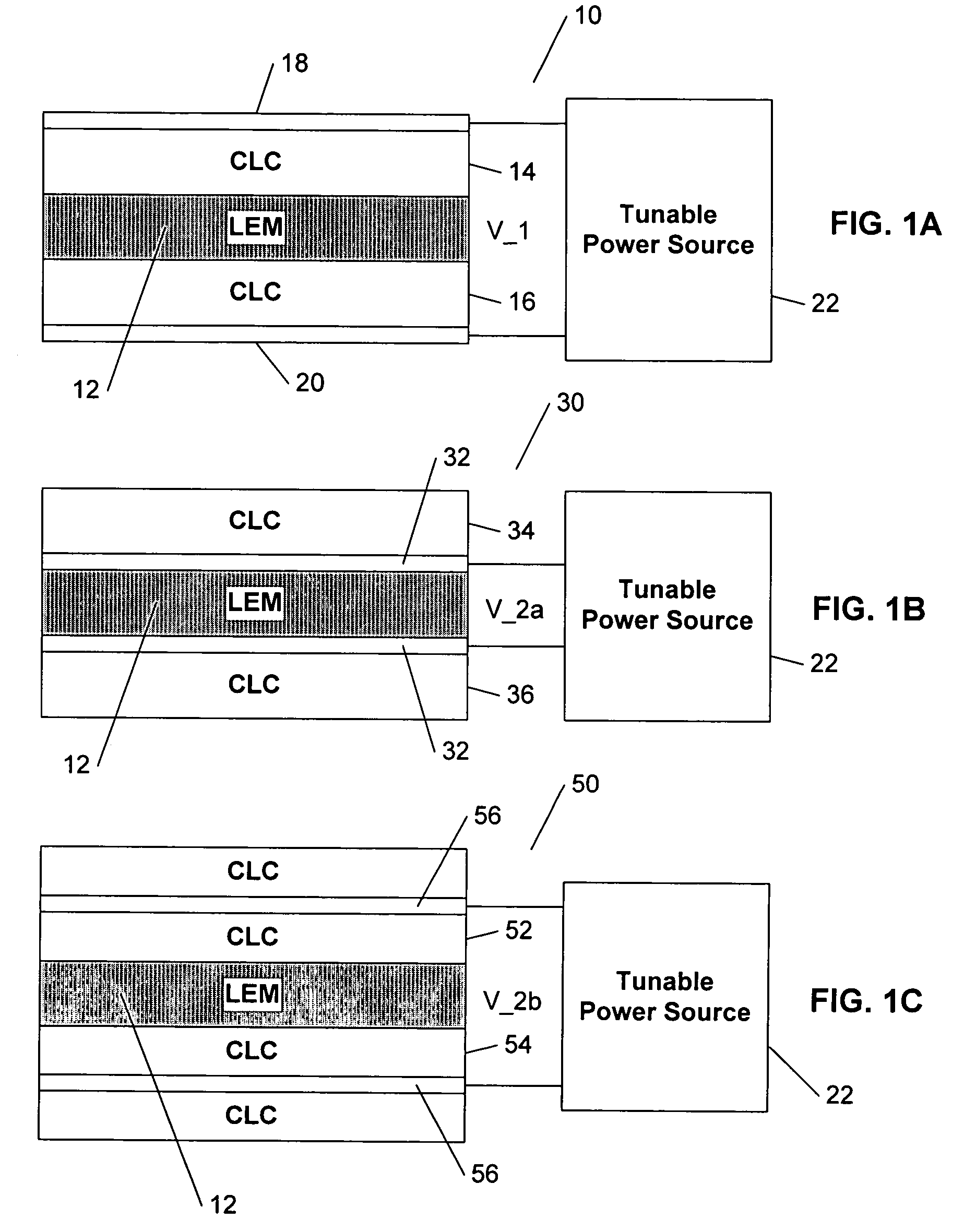
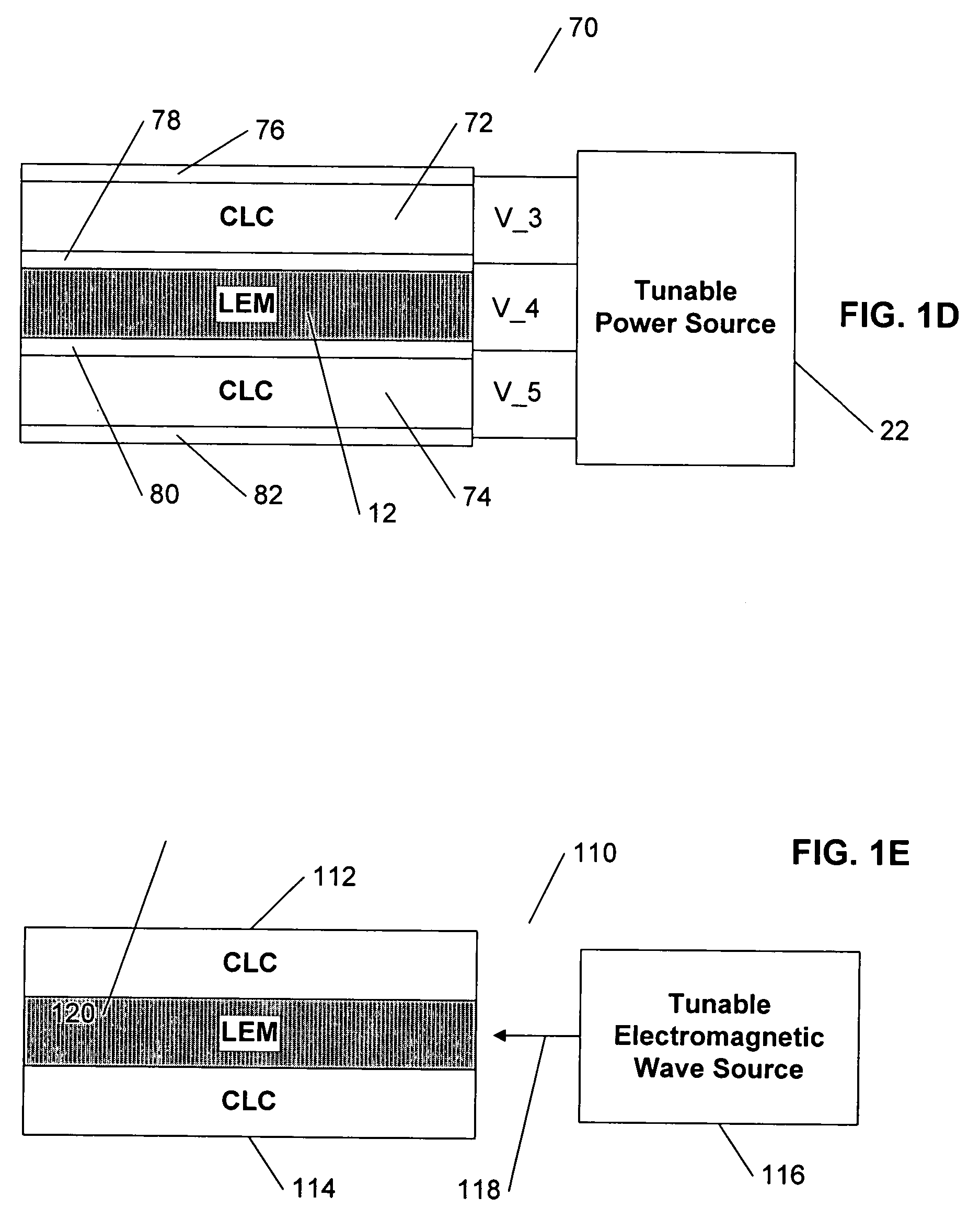
[0054]Referring initially to FIG. 1A, in the present invention, a wide-area coherent chiral laser 10 includes an active light-emitting material 12 for producing gain, such as a light-emitting diode (e.g. a GaAs diode), sandwiched between an upper cholesteric liquid crystal (“CLC”) layer 14 and a lower CLC layer 16. The light-emitting material 12 may include, but is not limited to: laser dyes, rare earth elements, conjugated polymers or any medium in which electron-hole recombination occurs in the active material. As noted above, the CLC layers 14 and 16 may be composed from any chiral substance capable of transmitting light.

[0055]A first electrode 18 is connected to the upper CLC layer 14 and a second electrode 20 is connected to the lower CLC layer 20. Both electrodes 18 and 20 are connected to an external electrical power source 22. The tunable power source 22 may be any tunable electrical current source capable of providing charge current between electrodes connected thereto. Opt...

second embodiment

[0059]Referring now to FIG. 1B, the invention is shown as a chiral laser 30. The chiral laser 30 includes an active light-emitting material 12 for producing gain, sandwiched between an upper CLC layer 34 and a lower CLC layer 36. As noted above, the CLC layers 34 and 36 may be composed from any chiral substance capable of transmitting light.

[0060]A first electrode 32 is positioned between the upper CLC layer 34 and the light-emitting material 12, while a second electrode 32 is positioned between the light-emitting material 12 and the lower CLC layer 36. Both electrodes 32 are connected to the external electrical power source 22. When a voltage V_2a is applied between electrodes 32 by the power source 22, a charge current passes through the light-emitting material 12, exciting it and causing spontaneous and stimulated emission of electromagnetic radiation that results in polarized lasing at a predefined lasing wavelength. Lasing occurs in a direction perpendicular to the CLC layers 3...

third embodiment

[0062]Referring now to FIG. 1C, the present invention is shown as a chiral laser 50. The chiral laser 50 includes an upper CLC layer 52, a light-emitting material layer 12, a lower CLC layer 54, a first electrode 56 embedded within the upper CLC layer 52 and a second electrode 56 embedded within the lower CLC layer 54. Both electrodes are connected to the power source 22. The chiral laser 50 operates substantially in a similar manner to the chiral laser 30 except that the electrodes 56 need not be as transparent as electrodes 32, and the CLC layers 52 and 54 must be conductive. The voltage V_2b applied by the power source 22 is between V_1 and V_2a. Thus, the chiral laser 50 is less sensitive to the transparency of the electrodes than the chiral laser 30, but requires a higher voltage and more complex fabrication techniques.


PUM

PropertyMeasurementUnit
thicknessaaaaaaaaaa
refractive indexaaaaaaaaaa
frequencyaaaaaaaaaa

Abstract

Lasing at the edge of the reflection band or at a defect state within the reflection band of a thin one-dimensional feedback structure is used to create a large-area, thin-film laser source with transverse dimensions that can be much greater than the film thickness. Angular confinement of radiation propagating perpendicular to the layers leads to a spreading of the beam inside the medium which is much greater than the diffraction divergence. This enhances the spatial extent of correlation at the output surface of the thin film. When a pump source induces gain at the lasing threshold in a wide region, a spatially coherent monochromatic light beam is emitted perpendicular to the film surface from the entire gain region. Alternate embodiments of the present invention include a passive spatial filter and an active amplifier.

Description

RELATED APPLICATIONS[0001]This application is a continuation-in-part (CIP) application claiming priority from co-pending U.S. patent application Ser. No. 09 / 755,859 entitled “Thin-Film Large-Area Coherent Light Source, Filter, and Amplifier Apparatus and Method” which was filed on Jan. 5, 2001 now abandoned, which in turn claims priority from U.S. Provisional Patent Application Ser. No. 60 / 175,007 entitled “Thin-Film Large-Area Coherent Light Source and Filter Apparatus and Method” which was filed on Jan. 7, 2000, and from U.S. Provisional Patent Application Ser. No. 60 / 182,125 entitled “Improved Thin-Film Large-Area Coherent Light Source and Filter Apparatus and Method” which was filed on Feb. 12, 2000.FIELD OF THE INVENTION[0002]The present invention relates generally to lasers based on feedback structures, and more particularly to large-area, thin-film laser sources that may be optionally utilized as filters and amplifiers.BACKGROUND OF THE INVENTION[0003]Semiconductor coherent l...

Claims


Application Information

Patent Timeline
Patent Type & Authority Patents(United States)
IPC IPC(8): H01S3/14G11B7/125H01S3/06H01S3/08H01S3/091H01S3/092H01S3/16H01S5/04H01S5/183H04N9/31
CPCG11B7/126H01S3/0604H01S3/08H04N9/3129H01S3/08009H01S3/08059H01S3/091H01S3/092H01S3/14H01S3/16H01S3/1603H01S3/168H01S3/1686H01S5/041H01S5/183
Inventor KOPP, VICTOR IL'ICHZHANG, ZHAO-QINGGENACK, AZRIEL ZELIG
Owner CHIRAL PHOTONICS
Learn More