Radio frequency doubler

a radio frequency doubler and frequency technology, applied in the field of high frequency doublers, can solve the problems of increasing the size of the circuit, increasing the current consumption, and not being applicable to an integrated circuit using a differential circuit, so as to achieve the effect of efficiently outputing only a double frequency and facilitating integration

Active Publication Date: 2007-07-17
PANNOVA SEMIC
View PDF11 Cites 5 Cited by
  • Summary
  • Abstract
  • Description
  • Claims
  • Application Information

AI Technical Summary

Benefits of technology

[0007]In view of the above problem, an object of the present invention is to efficiently extract a doubled signal with ease.
[0013]According to the circuit configuration of the present invention, it is possible to provide a circuit capable of readily performing integration and efficiently output only a double frequency merely by inputting a simple differential signal without the need for the original signal which has been phase controlled. Further, a DC short circuit in the resonance circuit makes it possible to eliminate a DC offset voltage in an output. A variable capacitance can be changed to vary a conversion gain relative to a desired double frequency. The output level of a doubled output can be changed by varying the level of the original signal inputted to the bases of the fifth and sixth transistors.

Problems solved by technology

This means that the output level of a signal with a double frequency is also changed, resulting in a problem in practical use.
However, the circuit size is increased by using such a circuit and current consumption also increases.
However, the circuit of JP2998773B shown in FIG. 4 is a single-phase circuit and thus is not applicable to an integrated circuit using a differential circuit.
Thus, the circuit is not applicable to a system requiring a high suppression level of the original signal.
In reality, an ideal multiplication is not performed due to asymmetry caused by variations between transistors.

Method used


Image

  • Radio frequency doubler
  • Radio frequency doubler
  • Radio frequency doubler

Examples


embodiment 1

[0019]The following will describe the circuit configuration of Embodiment 1 of the present invention in accordance with the accompanying drawings.

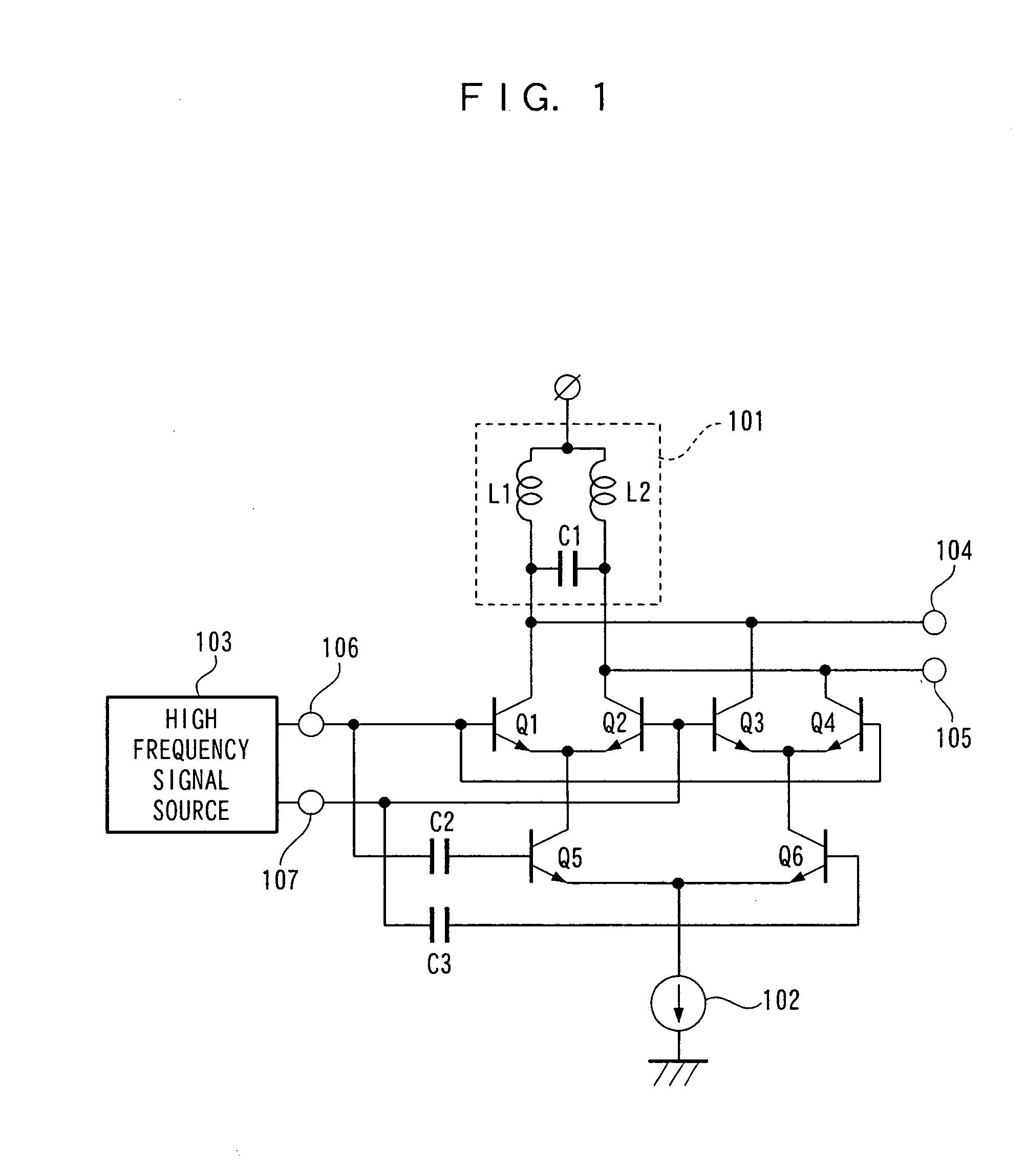
[0020]FIG. 1 is a circuit diagram showing electrical connection of an embodiment of a high frequency doubler according to the present invention. In FIG. 1, a high frequency signal source 103 indicates the original signal to be doubled and generates differential signals for output terminals 104 and 105. Signals from the signal source 103 are inputted to the bases of transistors Q1 and Q3 and the bases of transistors Q2 and Q4. At the same time, the signals are differentially inputted to transistors Q5 and Q6 via capacitors C2 and C3. At this moment, this circuit performs the same operation as a multiplier and a frequency doubled from that of the original signal is generated, as a differential output, at the collector terminals of the transistors Q1 and Q3 and the transistors Q2 and Q4. The original signal inputted then is not outputted acco...

embodiment 2

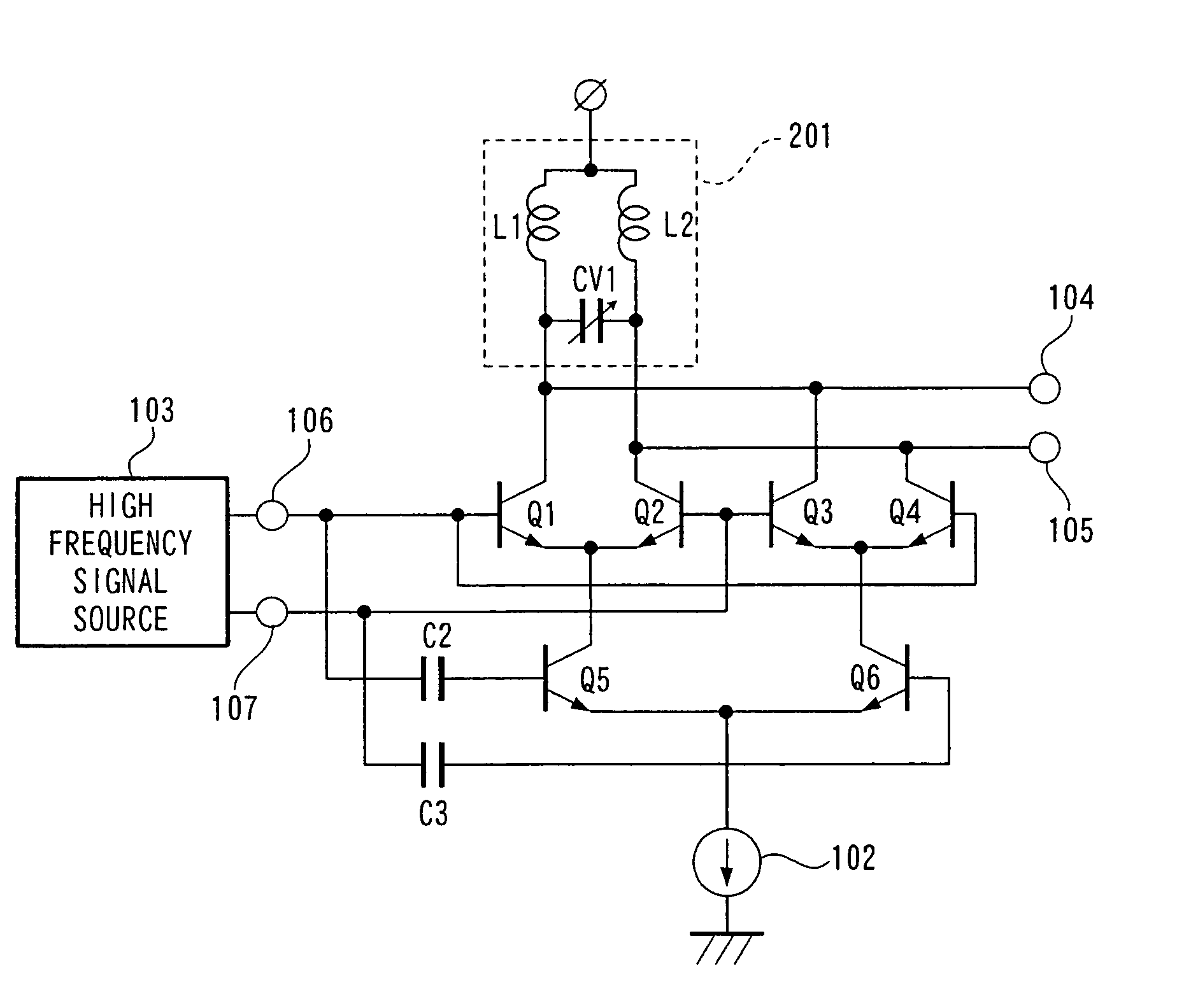
[0022]FIG. 2 is a circuit diagram showing electrical connection of an embodiment of a high frequency doubler according to claims 3 and 4 of the present invention. Basic operations are similar to those of the above-described invention and thus the explanation thereof is omitted. In the present invention, capacitances are changed in inductors L1 and L2 and a variable capacitance CV1, which determine a resonant frequency in a resonance circuit, so that a conversion gain is changed relative to a frequency twice as high as a desired frequency. In this case, resonance means a frequency enabling matching of an impedance which is output-connected. Therefore, impedances connected to output terminals 104 and 105 apparently change the values of a capacitance and the inductors L1 and L2 of a resonance circuit 201. Further, in the doubler of the present invention, not only a doubled input signal but also signals obtained by multiplying an input signal by even numbers of 4, 6, and so on are gener...

embodiment 3

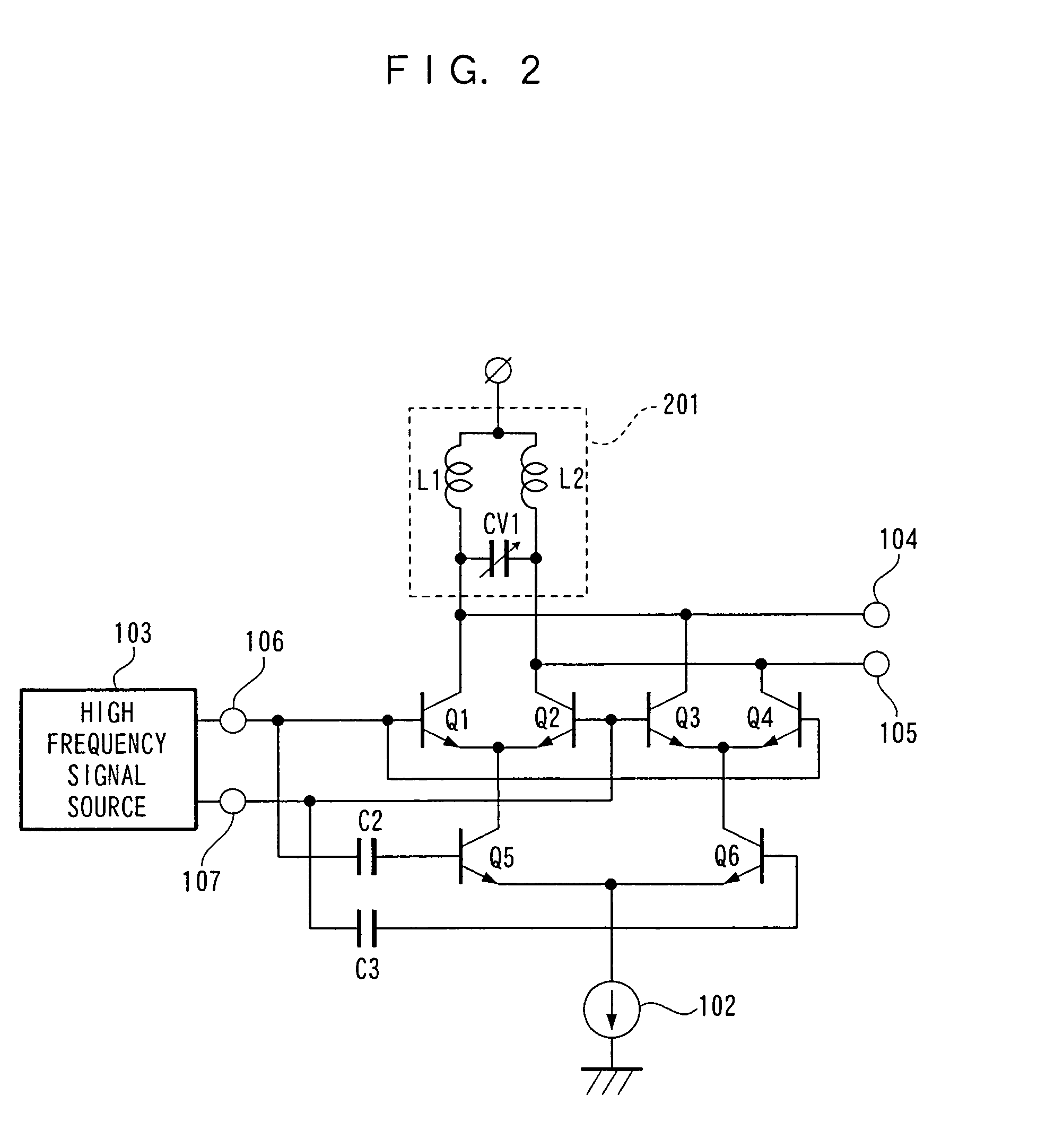
[0023]FIG. 5 shows an embodiment of a variable gain high frequency doubler according to claim 5 of the present invention. Basic operations are similar to those of Embodiment 1 and thus the explanation thereof is omitted. In the present invention, the level of the original signal inputted to the bases of fifth and sixth transistors Q5 and Q6 is changed by a variable attenuator 501, so that the output level of a doubled output can be changed. The same effect as the variable attenuator can be obtained by a variable gain unit 501.

[0024]In the high frequency doubler according to first to fifth inventions, the transistors can be any kind of field-effect transistors (FET) such as a MOSFET.


PUM


Abstract

When a signal of a double frequency is generated from the original signal, conventionally a 90-degree phase-shift circuit is necessary to suppress an output of a DC component and efficiently obtain a double wave. According to the present invention, an equal RF signal is inputted to input terminals and an output is matched with a frequency as high as that of the original frequency in a Gillbert cell double-balanced mixer, so that a doubled output is obtained with no DC offset. According to the circuit configuration of the present invention, it is possible to provide a circuit readily performing integration and to efficiently output only a double frequency merely by inputting a simple differential signal without the need for the original signal which has been phase controlled. Further, a DC short circuit in the resonance circuit makes it possible to eliminate a DC offset voltage in an output.

Description

FIELD OF THE INVENTION[0001]The present invention relates to a high frequency doubler in which a differential signal of a high frequency is supplied to the base of a transistor and a tuned circuit resonating at a frequency twice as high as a frequency of the original signal is connected to a collector terminal.BACKGROUND OF THE INVENTION[0002]In recent years, as communications speed up, frequencies used for mobile phones and so on have increased to the 1 GHz, 2 GHz, and 5 GHz bands. Thus, a technique for generating an RF frequency is important. As a solution for attaining the technique, a technique of multiplying a low frequency of the original signal to a desired frequency is available.[0003]Doublers frequently used as integrated circuits include an application of a Gillbert cell double-balanced mixer circuit, which uses a differential amplifier shown in FIG. 3. In this circuit, high frequency differential signals having been phase shifted from each other by 90 degrees are inputted...

Claims


Application Information

Patent Timeline
Patent Type & Authority Patents(United States)
IPC IPC(8): H03B19/00H03B19/14H03D7/14H03F3/45H03F3/34H04N9/68
CPCH03B19/14H03D7/1433H03D7/1441H03D7/1458H03B2200/0036H03B2200/0098H03D2200/0025H03D2200/0047
Inventor ITO, JUNJI
Owner PANNOVA SEMIC
Why Eureka
Try Eureka