

Glass-type planar substrate, use thereof, and method for the production thereof
a technology of planar substrate and glass, which is applied in the direction of glass shaping apparatus, decorative arts, chemical vapor deposition coating, etc., can solve the problems of narrow production limitations, limited glass structure possibilities, and very interesting products, and achieve good thermal compatibility of materials
- Summary
- Abstract
- Description
- Claims
- Application Information
AI Technical Summary
Benefits of technology
Problems solved by technology
Method used
Image

Examples
Embodiment Construction
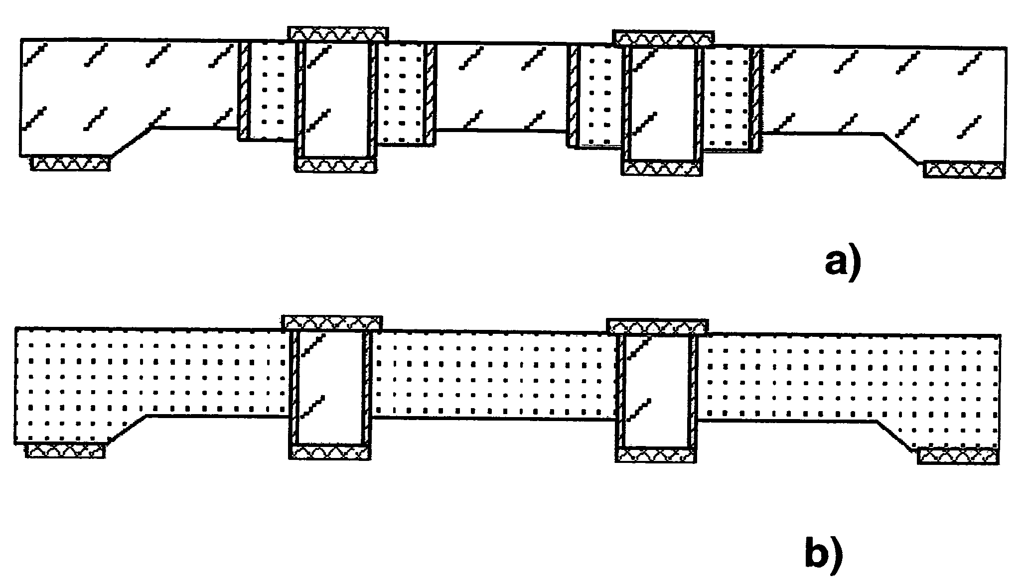
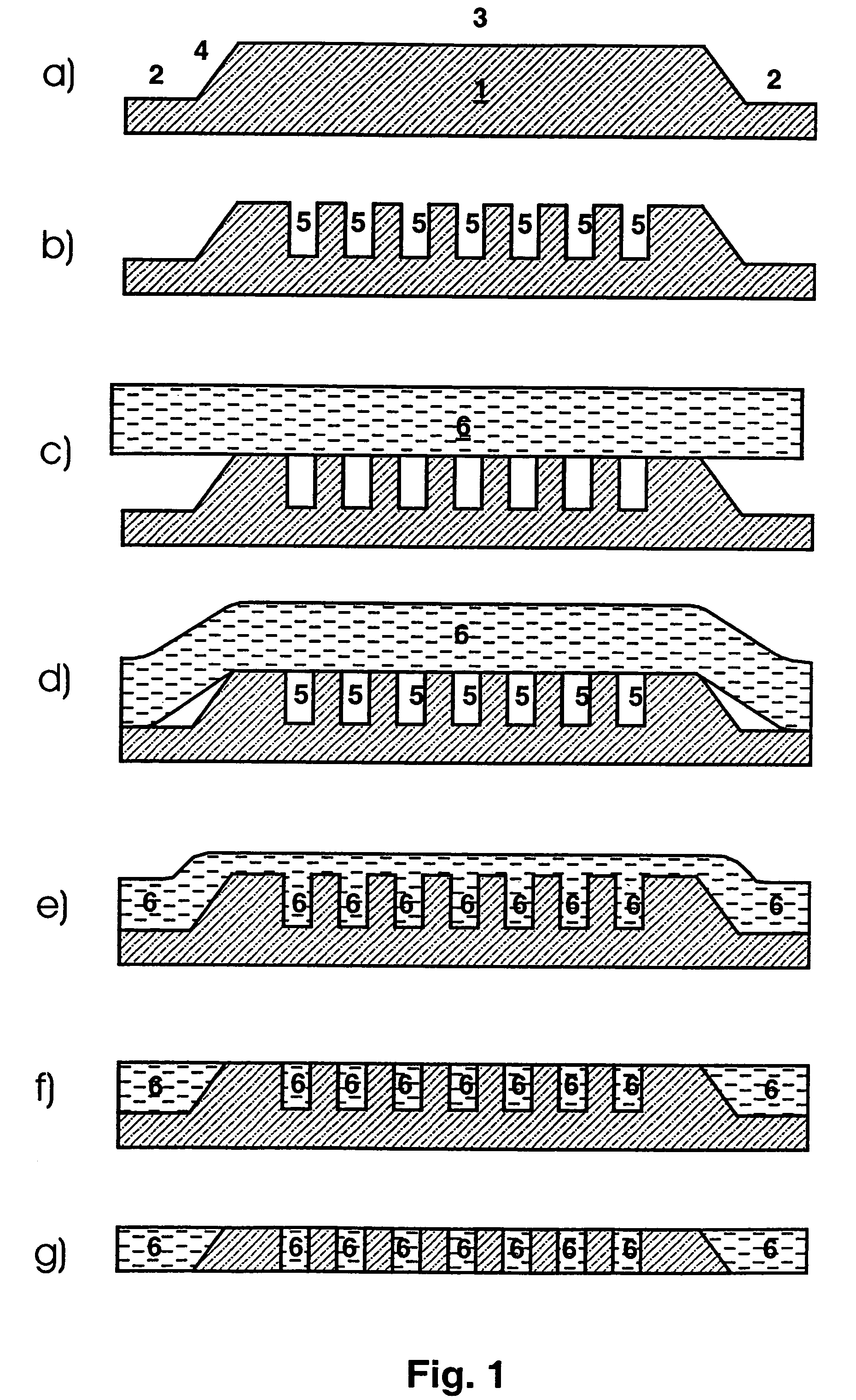
[0011]The object of the present invention is to further develop the method for structuring a planar surface made of a glasslike material described in DE 101 18 529 in such a manner that the costs of the method are substantially reduced. It should be possible to replace the etching process required for prestructuring the semiconductor planar surface with a less expensive structuring technique. Moreover, all the advantages that can be achieved with the method according to DE 101 18 529 should be retained without limitations.
[0012]The solution to the object of the present invention is set forth in claims 1 and 2. The subject matter of claim 33 is a glasslike planar substrate produced and structured using the present method. Furthermore, preferred applications of the products, that can be produced with the method, are described. The subject matter of the subordinate claims and the description, in particular with reference to the figures, relate to features that advantageously further de...
PUM
| Property | Measurement | Unit |
|---|---|---|
| thickness | aaaaa | aaaaa |
| edge width | aaaaa | aaaaa |
| thickness | aaaaa | aaaaa |
Abstract
Description
Claims
Application Information