Source synchronous CDMA bus interface

a synchronous cdma and bus interface technology, applied in the field of source synchronous cdma, can solve the problems of limiting system performance, bandwidth and latency of memory systems, and limiting system performance, so as to achieve high bus concurrency, improve signal integrity, and reduce channel latency

Inactive Publication Date: 2007-08-28
SILICON STORAGE TECHNOLOGY
View PDF9 Cites 19 Cited by
  • Summary
  • Abstract
  • Description
  • Claims
  • Application Information

AI Technical Summary

Benefits of technology

[0015]The present wireless interconnection system serves. to largely eliminate the bit rate and feature size limitations associated with conventional metal interconnects. In accordance with the present invention, interconnections are made between first and second IC locations via a wireless transmission medium. A signal to be conveyed from a first IC location to a second IC location is modulated, and the modulated signal is capacitively coupled to the wireless transmission medium. The modulated signal propagates through the wireless transmission medium, and is capacitively coupled to a receiver which demodulates the modulated signal and delivers the demodulated signal to the second IC location. The wireless medium is preferably either a microstrip data channel (MTL) or a coplanar waveguide (CPW), which is preferably terminated at both ends with an impedance equal to the medium's characteristic impedance ZC. The first and second IC locations may be on the same die or separate dies, such that either intra-chip or inter-chip interconnections are facilitated.
[0017]The present SS-CDMA bus interface utilizes source synchronous signaling and direct-sequence code-division multiple access (CDMA) techniques to provide high bus concurrency and low channel latency. The interface is re-configurable, and provides multi-chip access for applications in high-bandwidth multi-drop parallel interconnections such as a memory bus without increasing the number of independent channels or different DRAM banks.
[0018]The new interface employs direct-sequence spread spectrum (DS-SS) multiple access schemes, which enable two or more separate data bits be sent through the same channel simultaneously and successfully recovered at the receiver. The present bus interface is suitably employed in a wired multi-drop memory bus system based on 3-PAM signaling with source synchronous clocking to simultaneously send two bits of data through one PCB channel. By decreasing the number of channels required, signal integrity is improved and interface power consumption is reduced. Further, higher performance and lower bus interface costs are achieved due to the use of fewer pins and PCB channels, smaller die and package size, and simplified PCB design.

Problems solved by technology

Thus, chip-to-chip communication speed usually limits system performance.
In particular, the bandwidth and latency of memory systems have been limiting factors for system performance.
However, the approaches taken by these RAM systems—which each rely on a traditional memory bus interface—can only do so much, as they are designed for system architectures having many sources of overhead.
The costs associated with DRAM memories increases with the number of I / O pins on the DRAM package.
However, both these approaches increase cost; furthermore, channel latency and concurrency problems still exist. FIGS. 1(a) and 1(b) show two typical primary memory bus configurations, in which n DRAM chips 10 are connected to a common data bus 12 and to an address / control bus 14, and the bus lines are connected to a CPU 16 and a memory controller 18 interconnected as shown.
If these configurations utilize a conventional memory bus, such as the high-speed narrow channels used in D-RDRAM, they suffer from long channel latency: for instance, if two read requests arrive at DRAM1 back-to-back or two read requests arrive at DRAM1 and DRAM2, respectively, the second request must stall until the first request finishes using the shared data bus.
But, high frequency parallel lines create crosstalk noise and degrade signal integrity.
However, this causes the die size and package size to increase, and thus complicates PCB design.
Other memory bus systems have attempted to solve the problems of high-speed access to memory with limited success.
However, under this approach, the number of I / O pins must increase with the size of the DRAM, with the pin count possibly becoming unacceptably large with the high capacities of modern-day DRAM chips.
However, though D-RDRAMs can reduce the number of I / O pins needed by using a high speed bus interface, they typically require a number of shielding pins to reduce the cross-talk noise and inter-symbol interference (ISI) effects on the PCB board.
D-RDRAMs may also require a 184 pin package, which increases chip cost.
As a result, the parasitic resistance, capacitance and inductance associated with an IC's wires are beginning to adversely affect circuit performance, and have increasingly become a primary stumbling block in the evolution of deep sub-micron ultra-LSI (ULSI) technology.
Recent studies have indicated that when feature sizes fall below 1 μm, the interconnect parasitics cause signal attenuation and dispersion in the wires, seriously hurting circuit and system performance.
The RC (or LC) time delay, IR voltage drop, CV2f power loss and crosstalk parameters of an IC's wires also become significant at higher bit rates.
Nevertheless, these evolutionary approaches may soon encounter fundamental material limits which will inhibit further feature size reductions and / or bit rate increases.

Method used


Image

  • Source synchronous CDMA bus interface
  • Source synchronous CDMA bus interface
  • Source synchronous CDMA bus interface

Examples


Embodiment Construction

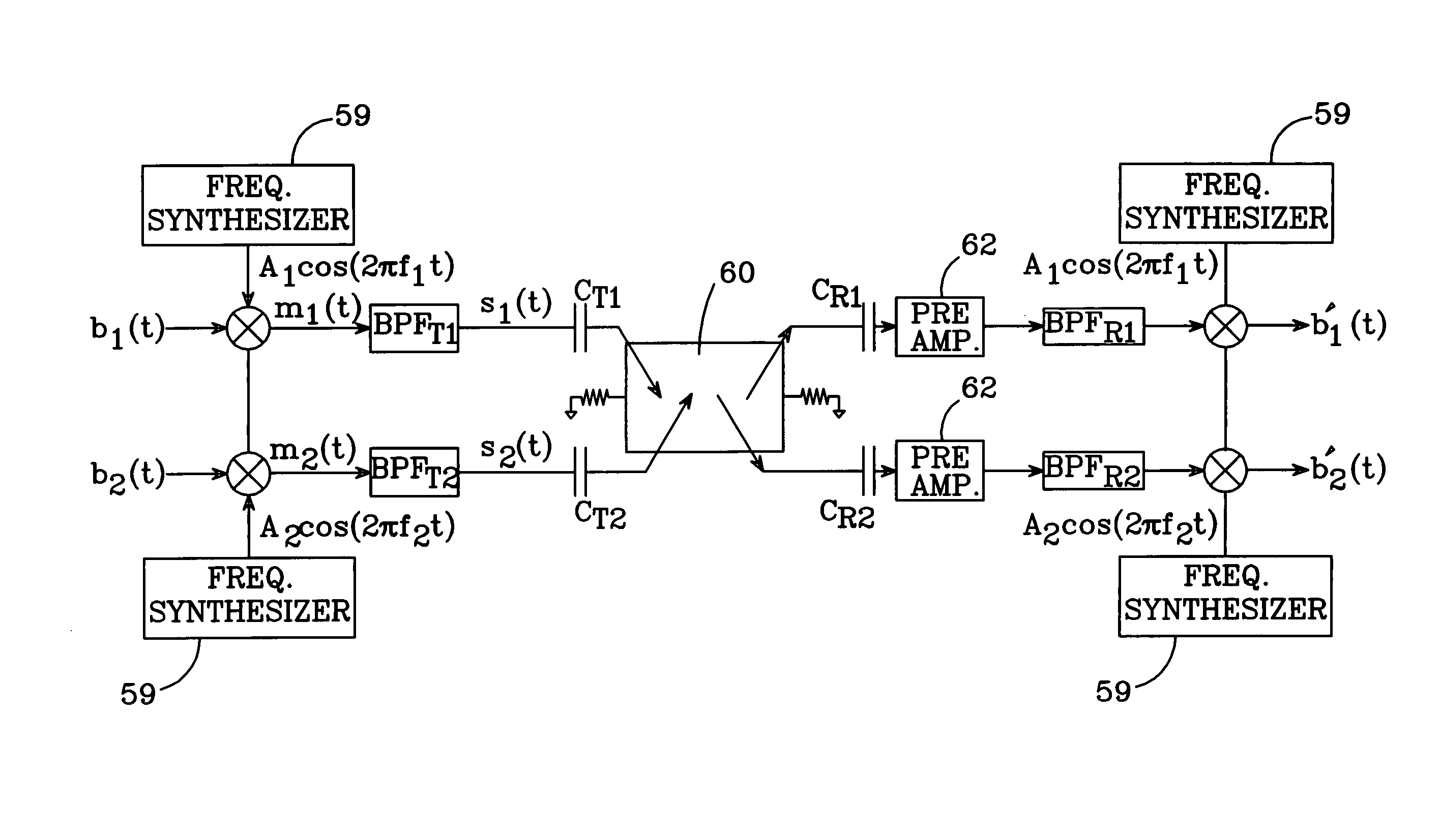
[0046]The basic principles of a wireless interconnection system in accordance with the present invention are shown in FIGS. 3a and 3b, which show plan and corresponding cross-sectional views of a package 10 which employs the present invention. The package includes two integrated circuits ULSI-A and ULSI-B which require interconnection. In this example, ULSI-A produces a signal which must be conveyed to ULSI-B. Conventionally, such a signal would be conveyed via a metal interconnect or a wire bond. Here, however, the signal is conveyed wirelessly. The signal from ULSI-A is modulated and routed to a first capacitive coupler 12, which capacitively couples the signal to a wireless transmission medium 14. The wireless transmission medium is physically separated from the ICs, and the ICs separated from each other, with a dielectric filler material 16.

[0047]The capacitively coupled signal propagates through wireless transmission medium 14. A second capacitive coupler 18 couples the propaga...


PUM


Abstract

A wireless IC interconnect system and a source synchronous CDMA (SS-CDMA) bus interface facilitate interconnections between first and second IC locations. A signal conveyed using the wireless system is modulated and capacitively coupled to a transmission medium, and then capacitively coupled from the medium to a receiver which demodulates the modulated signal and provides the demodulated signal to the second IC location. Multiple signals can be conveyed simultaneously by modulating and demodulating them using multiple access algorithms such as CDMA and / or FDMA. The SS-CDMA bus interface utilizes source synchronous signaling and CDMA techniques to provide high bus concurrency and low channel latency. The interface is re-configurable, and provides multi-chip access in high-bandwidth multi-drop parallel interconnection applications. The interface employs spread spectrum multiple access schemes, which enable two or more data bits to be sent through the same channel simultaneously and successfully recovered at the receiver.

Description

CROSS-REFERENCE TO RELATED APPLICATIONS[0001]This application is a continuation-in-part of application Ser. No. 09 / 839,107, filed Apr. 20, 2001 now U.S. Pat. No. 6,856,788.BACKGROUND OF THE INVENTION[0002]1. Field of the Invention[0003]This invention relates to the field of integrated circuit (IC) interconnections, and particularly to wired and wireless systems and methods of effecting inter- and intra-chip interconnections.[0004]2. Description of the Related Art[0005]Chip-to-chip communications—i.e., the transfer of data between different ICs within a system—are under ever-increasing pressure to perform faster. This is particularly true for bus-based communications between a CPU and RAM in a computer system.[0006]The traditional chip-to-chip communication speed on a printed circuit board (PCB) is usually much lower than the speed of a CPU. Thus, chip-to-chip communication speed usually limits system performance. In particular, the bandwidth and latency of memory systems have been l...

Claims


Application Information

Patent Timeline
Patent Type & Authority Patents(United States)
IPC IPC(8): H04L7/00H04B5/02
CPCH04B5/0012H04B5/02
Inventor CHANG, MAU-CHUNG F.KIM, JONGSUN
Owner SILICON STORAGE TECHNOLOGY
Why Eureka
Try Eureka