
Integrated circuit apparatus

a circuit apparatus and integrated circuit technology, applied in the field of integrated circuit apparatuses, can solve the problems of increasing the number of latches, the problem of latches still remaining, and the inability to latch up, so as to avoid the effect of data loss, facilitate the recovery of lost data, and limit the range of data loss

Inactive Publication Date: 2007-09-25
RENESAS ELECTRONICS CORP
View PDF7 Cites 8 Cited by
  • Summary
  • Abstract
  • Description
  • Claims
  • Application Information

AI Technical Summary

Benefits of technology

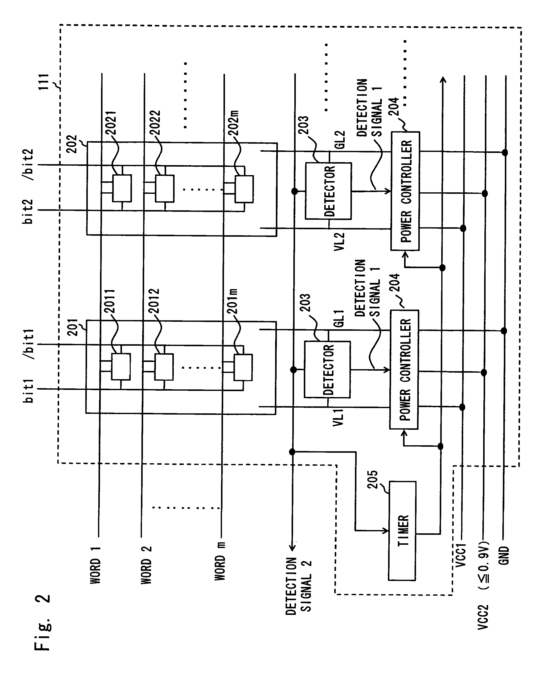
[0017]According to another aspect of the present invention, there is provided an integrated circuit apparatus that includes a static random access memory (SRAM) cell array including a plurality of memory cells formed of complementary field effect transistors arranged lattice-like, a power line placed in each 1-bit sequence of the SRAM cell array, a detector detecting occurrence of an effect of a parasitic bipolar transistor or a snap-back effect that is similar thereto for each 1-bit sequence and outputting a detection signal, and a power controller controlling a voltage to be supplied to the power line for each 1-bit sequence. The power controller reduces a voltage to be supplied to the power line placed in a 1-bit sequence where the occurrence of an effect of a parasitic bipolar transistor or a snap-back effect that is similar thereto is detected by the detector down to a predetermined value according to the detection signal.
[0019]The integrated circuit apparatus of the present invention having the above configuration can limit the range that is affected by the effect of a parasitic bipolar element such as latch-up or a snap-back effect similar thereto to the range of a 1-bit sequence of the SRAM cell array. Further, since it is possible to limit the range where data is lost due to the effect of a parasitic bipolar element such as latch-up or a snap-back effect similar thereto, it facilitates the recovery of lost data by ECC processing.
[0021]This configuration allows recovering the data lost by the effect of a parasitic bipolar device such as latch-back or a snap-back effect similar thereto by ECC processing. It is therefore possible to avoid the affect of data loss due to latch-up or other effects of a parasitic bipolar device or a snap-back effect in an integrated circuit apparatus having an SRAM cell array formed of CMOSFET.
[0022]The present invention can reduce the effects of data loss due to latch-up or other effects of a parasitic bipolar device or a snap-back effect of MOSFET that is similar thereto in an integrated circuit apparatus having an SRAM cell array formed of CMOSFET.

Problems solved by technology

An integrated circuit having a complementary metal oxide semiconductor field effect transistor (CMOSFET) is susceptible to latch-up that an abnormal current flows between a power supply and a ground of the integrated circuit, caused by a parasitic bipolar transistor with a thyristor structure in CMOSFET turning ON upon application of an overvoltage to an input / output terminal or the like.
At the same time, since a PN isolation interval decreases due to the miniaturization of an integrated circuit, the ability of a parasitic bipolar transistor that causes latch-up increases and therefore the problem of latch-up still remains.
Further, since a gate length of MOSFET also decreases like in the parasitic bipolar, snap-back behavior is also likely to occur at a low voltage.
The problem of latch-up is particularly serious in an SRAM cell array that is composed of CMOS memory cells with a low density of a well potential contact and a substrate potential contact.
Occurrence of latch-up in the SRAM cell array leads to not only breakdown of the data stored in the memory cell but also hard errors if the latch-up is left unsolved.
Thus, even if hard errors are avoided by placing a detector between the power line and ground line to detect latch-up and blocking power supply, data of the entire memory cells affected by latch-up can be lost.
If latch-up occurs in such a cell array, the data retained in the entire memory cells of the 8-bit sequence supplied with power through the pair of power supply line and ground line is lost.

Method used


Image

  • Integrated circuit apparatus
  • Integrated circuit apparatus
  • Integrated circuit apparatus

Examples


first embodiment

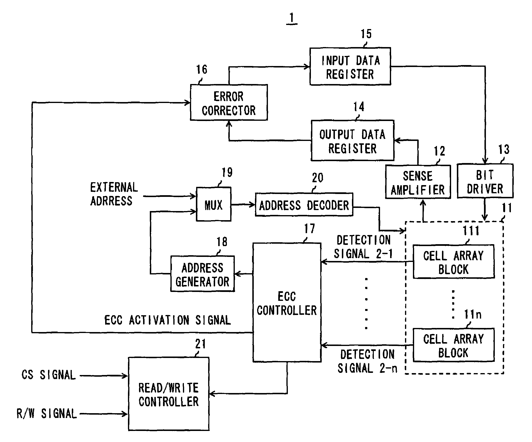
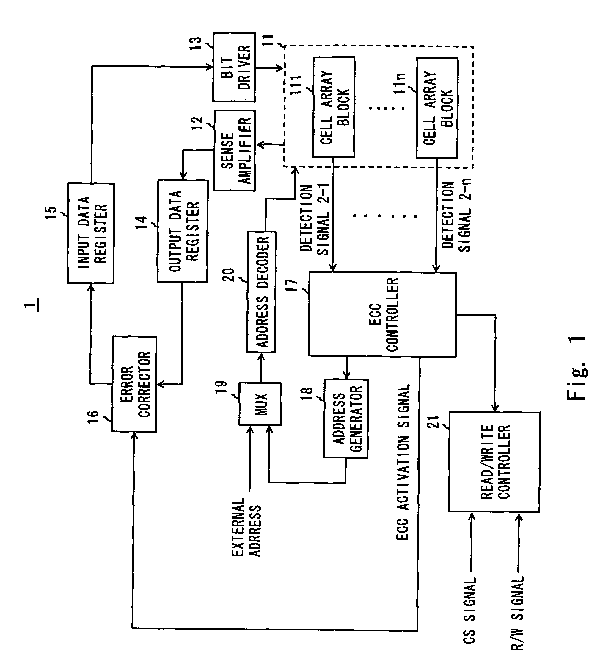
[0032]FIG. 1 shows the configuration of an integrated circuit apparatus 1 according to an embodiment of the present invention. A cell array 11 is an SRAM cell array where memory cells formed of CMOSFET are arranged lattice-like. The cell array 11 is divided into one or a plurality of cell array blocks 111 to 11n. Each of the cell array blocks has a configuration where memory cells are arranged lattice-like, and each memory cell is connected to a word line (row selection line) and a bit line (column selection line). The detailed configuration of the cell array block 111 of this embodiment is described later. A sense amplifier 12 and a bit driver 13 are connected to a bid line of the cell array 11. In data reading, the sense amplifier 12 detects and amplifies information of the memory cell and stores the read data into an output data register 14. In data writing, the bid driver 13 is driven according to information of input data register 15 and writes data to the memory cell.

[0033]The...

second embodiment

[0057]FIG. 7 shows the configuration of an integrated circuit apparatus 2 according to another embodiment of the present invention. The integrated circuit apparatus 2 is different from the integrated circuit apparatus 1 of the first embodiment in having a WAIT signal output circuit 22. The WAIT signal output circuit 22 supplies a WAIT signal to an external CPU or the like during error correction by ECC processing in order to notify the external CPU or the like that the error correction is currently being performed. The WAIT signal is a signal for indicating an external CPU or the like to wait without memory access.

[0058]The timing to output the WAIT signal may be set by indicating the output of the WAIT signal to the WAIT signal output circuit 22 in accordance with the timing when the ECC controller 17 outputs an ECC activation signal to indicate the data recovery to the error corrector 16. The functions of the other components of the integrated circuit apparatus 2 are the same as t...


PUM


Abstract

An integrated circuit apparatus includes a SRAM cell array having a plurality of memory cells formed of CMOSFET arranged lattice-like. The SRAM cell array has a pair of power line and ground line in each of 1-bit sequences. The integrated circuit apparatus also includes a detector detecting the occurrence of latch-up for each 1-bit sequence and outputting a detection signal, and a power controller controlling a power supply voltage to the power line for each 1-bit sequence. The power controller reduces a voltage to be supplied to the power line in the 1-bit sequence where latch-up is occurring down to a predetermined value according to the detection signal.

Description

BACKGROUND OF THE INVENTION[0001]1. Field of the Invention[0002]The present invention relates to an integrated circuit apparatus having an SRAM cell array formed of CMOSFET and, particularly, to an integrated circuit apparatus capable of reducing the effects of latch-up that occurs in an SRAM cell array.[0003]2. Description of Related Art[0004]An integrated circuit having a complementary metal oxide semiconductor field effect transistor (CMOSFET) is susceptible to latch-up that an abnormal current flows between a power supply and a ground of the integrated circuit, caused by a parasitic bipolar transistor with a thyristor structure in CMOSFET turning ON upon application of an overvoltage to an input / output terminal or the like.[0005]The reduction in a power supply voltage with miniaturization of an integrated circuit and the implementation of shallow trench isolation (STI) for device isolation have contributed to the improvement in latch-up resistance. At the same time, since a PN i...

Claims


Application Information

Patent Timeline
Patent Type & Authority Patents(United States)
IPC IPC(8): G11C5/14G11C7/00
CPCG11C5/147G11C11/417
Inventor FURUTA, HIROSHISHIMOGAWA, KENJYUMIZUGUCHI, ICHIROUMONDEN, JUNJITAKEDA, SHINJI
Owner RENESAS ELECTRONICS CORP
Learn More