High-temperature stable gate structure with metallic electrode

a gate structure and high-temperature stable technology, applied in the direction of basic electric elements, electrical equipment, semiconductor devices, etc., can solve the problems of physical vapor deposition methods falling into disfavor, prior forming methods have been unsuccessful in providing uniform, continuous and uniform ultra-thin high-k gate dielectric layers

a gate structure and high-temperature stable technology, applied in the direction of basic electric elements, electrical equipment, semiconductor devices, etc., can solve the problems of physical vapor deposition methods falling into disfavor, prior forming methods have been unsuccessful in providing uniform, continuous and uniform ultra-thin high-k gate dielectric layers

US7279413B2Inactive Publication Date: 2007-10-09GLOBALFOUNDRIES INC

Image

  • High-temperature stable gate structure with metallic electrode
  • High-temperature stable gate structure with metallic electrode
  • High-temperature stable gate structure with metallic electrode

Examples


Embodiment Construction

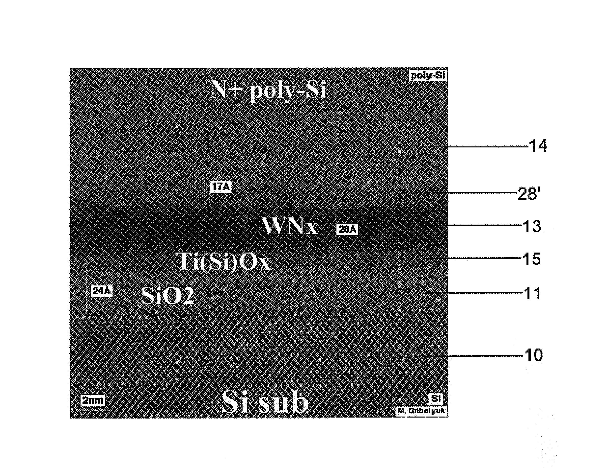
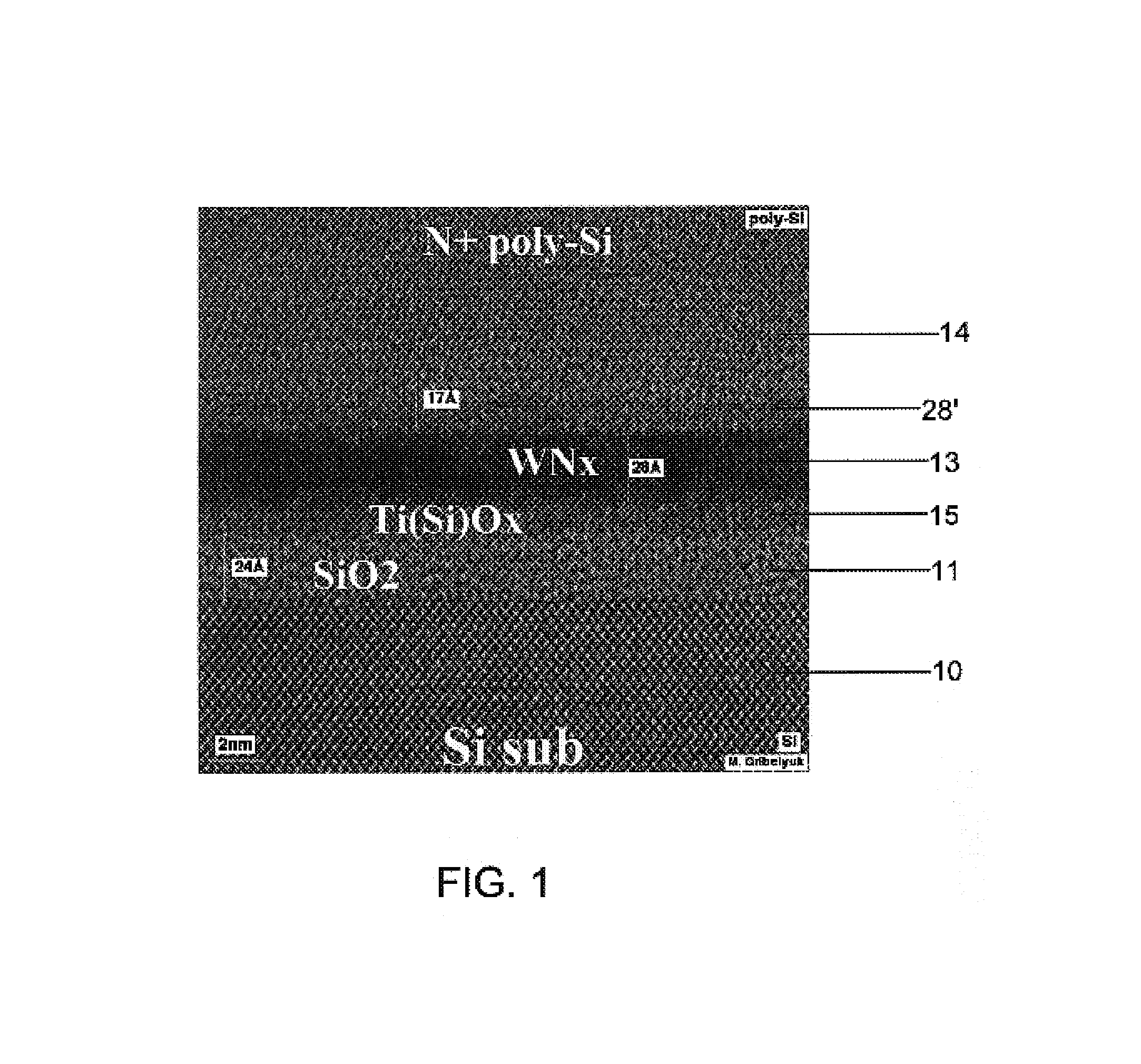
[0039]The present invention provides high-k gate dielectrics comprising uniform continuous ultra-thin high-k metal oxide layers, and a method of forming the same. The present invention advantageously provides a continuous ultra-thin high-k metal oxide layer by depositing a highly reactive layer of metal atoms atop a dielectric surface comprising at least silicon and oxygen atoms and forming an oxygen diffusion barrier atop the layer of metal atoms, in which the highly reactive layer of metal atoms and the oxygen diffusion barrier are formed in a non-oxidizing atmosphere. Following the deposition of a gate conductor atop the oxygen diffusion barrier, the highly reactive metal atom layer completely reacts with the dielectric surface to provide a continuous ultra-thin high-k metal oxide layer during subsequent annealing. Specifically, the metal atoms of the layer of metal atoms bonds with the oxygen atoms of the dielectric layer, thus converting the upper surface of the dielectric laye...


PUM

PropertyMeasurementUnit
dielectric constantaaaaaaaaaa
threshold voltageaaaaaaaaaa
temperatureaaaaaaaaaa

Abstract

The present invention provides a method for depositing a dielectric stack comprising forming a dielectric layer atop a substrate, the dielectric layer comprising at least oxygen and silicon atoms; forming a layer of metal atoms atop the dielectric layer within a non-oxidizing atmosphere, wherein the layer of metal atoms has a thickness of less than about 15 Å; forming an oxygen diffusion barrier atop the layer of metal atoms, wherein the non-oxidizing atmosphere is maintained; forming a gate conductor atop the oxygen diffusion barrier; and annealing the layer of metal atoms and the dielectric layer, wherein the layer of metal atoms reacts with the dielectric layer to provide a continuous metal oxide layer having a dielectric constant ranging from about 25 to about 30 and a thickness less than about 15 Å.

Description

RELATED APPLICATION[0001]This application is related to co-pending and co-assigned U.S. application Ser. No. 10 / 710,063 entitled TEMPERATURE STABLE METAL NITRIDE GATE ELECTRODE, filed on the same date. The entire content of this related application is incorporated by reference.FIELD OF THE INVENTION[0002]The present invention relates to a method for forming gate dielectrics, and more particularly, to a method for depositing a continuous high-k dielectric having a thickness on the order of about 15 Å or less. The term “high-k” denotes a dielectric material that has a dielectric constant of about 20 or greater. The term “continuous” denotes a continuously present layer of dielectric material, free of island growth.BACKGROUND OF THE INVENTION[0003]With decreasing gate lengths in metal oxide semiconductor field effect transistors (MOSFET), thin dielectrics are necessary to increase drive current and improve short channel behavior.[0004]Conventional methods for forming high-k dielectrics...

Claims


Application Information

Patent Timeline
09 Oct 2007
Publication
US7279413B2
IPC
H01L21/4763; H10B12/00; H01L21/28; H01L21/336; H01L21/44; H01L29/49; H01L29/51
CPC
H01L21/28088; H01L21/28176; H01L21/28185; H01L29/4966; H01L29/513; H01L21/28229; H01L29/66545; H01L29/517
Inventors
PARK, DAE-GYU; GLUSCHENKOV, OLEG G.