Interacting current spreader and junction extender to increase the voltage blocked in the off state of a high power semiconductor device

a technology of high-power semiconductor devices and current spreaders, which is applied in the direction of semiconductor devices, semiconductor/solid-state device details, electrical equipment, etc., can solve the problems of limited applications using high-power semiconductor devices, and achieve the effects of reducing manufacturing time and cost, simple implementation, and reducing current concentration

Active Publication Date: 2007-12-04
ARMY US SEC THE
View PDF18 Cites 63 Cited by
  • Summary
  • Abstract
  • Description
  • Claims
  • Application Information

AI Technical Summary

Benefits of technology

[0010]Another aspect of the invention provides a method of spreading current flowing in a semiconductor device, wherein the method comprises forming an electrode adjacent to a drift region, implanting a junction termination extension implant region in the drift region, positioning a current spreader adjacent to the junction termination extension implant region, and applying voltage to the semiconductor device resulting in a flow of current in the semiconductor device, wherein the step of positioning reduces a concentration of the current in an area connecting the electrode with the drift region. Furthermore, the step of positioning reduces current densities and electrostatic fields (preferably simultaneously) in the area connecting the electrode with the drift region. Also, the step of positioning spreads current flowing from the electrode into the drift region. The method further comprises connecting an ohmic metal contact to the electrode and configuring an implant pocket in the drift region, wherein the implant pocket is adapted for terminating electrostatic field lines in the semiconductor device. Preferably, the current spreader comprises an ohmic metal and the electrode comprises any of an anode and a cathode.
[0011]The embodiments of the invention achieve several advantages including that the embodiments of the invention are simple to implement because the fabrication processes for depositing the ohmic contact can also be used to deposit the current spreader. As such, no additional mask plates are needed, thereby reducing manufacturing time and costs. Furthermore, the embodiments of the invention increase the voltage blocked in high power semiconductor devices compared to conventional techniques for increasing the blocked voltage.
[0012]The embodiments of the invention are particularly advantageous in wide bandgap semiconductor devices, and more particularly, the embodiments of the invention may be utilized in silicon high-voltage product lines, with a potential use for these techniques in high power semiconductor devices made from silicon carbide (SiC) and other wide bandgap semiconductors including AlGaN. SiC and other wide bandgap materials tend to offer several advantages including the ability to operate bipolar devices at temperatures above 300° C., faster switching than silicon devices, and the ability to block higher voltages with thinner materials such that fewer devices are needed in series.
[0013]In particular, the SiC or other wide bandgap semiconductor material based devices that will benefit greatly from the field termination techniques provided by the embodiments of the invention include, but are not limited to, p-i-n diodes, IGBTs, thyristors, transistors and, in particular, any semiconductor device that would use a JTE to increase the voltage blocked in reverse bias. The above-mentioned devices are high power switches and are optimized for low leakage current when biased with a high reverse voltage (off state) and high current conduction with low applied forward voltage. Also, high frequency modulators requiring high reverse blocking can advantageously make use of the embodiments of the invention.

Problems solved by technology

However, applications using high power semiconductor devices may have been limited because of the lack of a p-n junction in silicon bipolar power devices when operating above 150° C. as is easily reached when handling high powers.
Both cases are inferior because thicker drift regions lead to slow switching, and having several devices in series may cause reliability problems unless the devices are identical and display the same characteristics over time.

Method used


Image

  • Interacting current spreader and junction extender to increase the voltage blocked in the off state of a high power semiconductor device
  • Interacting current spreader and junction extender to increase the voltage blocked in the off state of a high power semiconductor device
  • Interacting current spreader and junction extender to increase the voltage blocked in the off state of a high power semiconductor device

Examples


Embodiment Construction

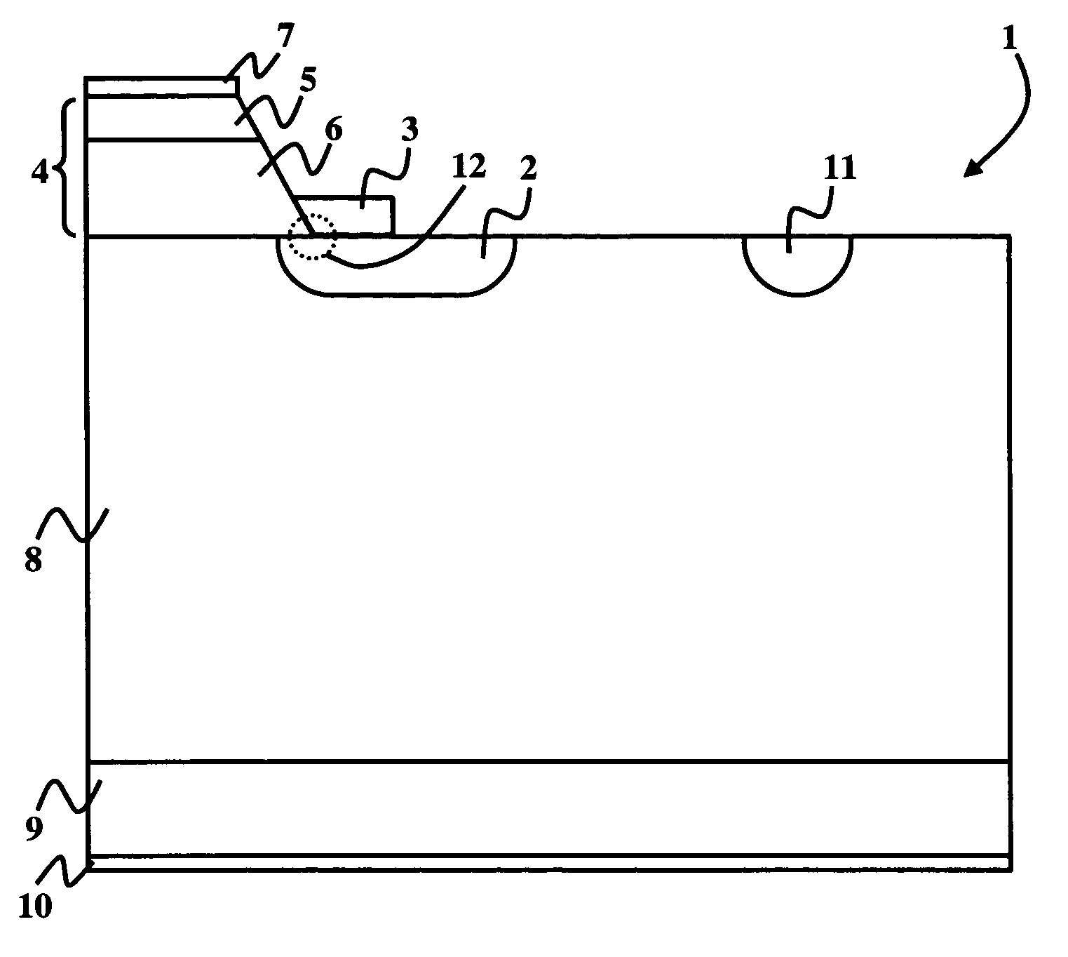
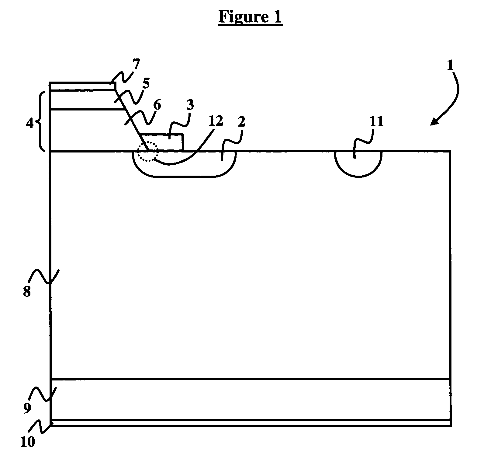
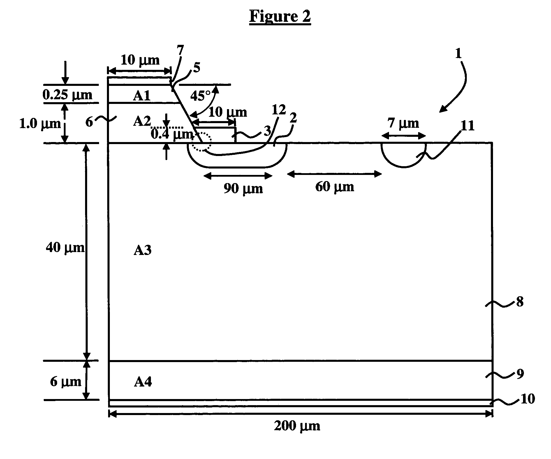
[0027]The embodiments of the invention and the various features and advantageous details thereof are explained more fully with reference to the non-limiting embodiments that are illustrated in the accompanying drawings and detailed in the following description. It should be noted that the features illustrated in the drawings are not necessarily drawn to scale. Descriptions of well-known components and processing techniques are omitted so as to not unnecessarily obscure the embodiments of the invention. The examples used herein are intended merely to facilitate an understanding of ways in which the embodiments of the invention may be practiced and to further enable those of skill in the art to practice the embodiments of the invention. Accordingly, the examples should not be construed as limiting the scope of the embodiments of the invention.

[0028]As previously mentioned, there remains a need for a novel high power semiconductor device that achieves high voltage blocking with low on-...


PUM


Abstract

A technique of spreading current flowing in a semiconductor device comprising an electrode, a drift region adjacent to the electrode, a junction termination extension implant region in the drift region, and a current spreader adjacent to the junction termination extension implant region and the electrode. The current spreader is adapted to reduce current densities and electrostatic fields (preferably simultaneously) in an area connecting the electrode with the drift region. Moreover, the current spreader is adapted to spread current flowing from the electrode into the drift region. The semiconductor device further comprises an ohmic metal contact connected to the electrode and an implant pocket in the drift region, wherein the implant pocket is adapted for terminating electrostatic field lines in the semiconductor device. Preferably, the current spreader comprises an ohmic metal and the electrode comprises any of an anode and a cathode.

Description

GOVERNMENT INTEREST[0001]The invention described herein may be manufactured, used, and / or licensed by or for the United States Government.BACKGROUND OF THE INVENTION[0002]1. Field of the Invention[0003]The invention generally relates to high power semiconductor devices, and more particularly to field termination structures used for enhancing voltage blocking abilities of semiconductor devices.[0004]2. Description of the Related Art[0005]Several field termination structures and techniques are presently utilized in the industry. These include field plates, field rings, beveling, and surface implant termination or junction termination extension (JTE) and they all tend to increase the voltage blocking ability of semiconductor devices. As known to those skilled in the art, field plates are metal contacts that do not conduct but instead alter the surface potential to reduce the curvature of electrostatic fields at the surface of the semiconductor device. Usually, the field plates are isol...

Claims


Application Information

Patent Timeline
Patent Type & Authority Patents(United States)
IPC IPC(8): H01L23/58
CPCH01L29/0615H01L29/861H01L29/8613H01L29/41H01L29/0619H01L29/868
Inventor SHAH, PANKAJ B.
Owner ARMY US SEC THE
Why Eureka
Try Eureka