Eureka AIR delivers breakthrough ideas for toughest innovation challenges, trusted by R&D personnel around the world.

Film-forming method, method of manufacturing semiconductor device, semiconductor device, method of manufacturing display device, and display device

a technology of semiconductor devices and film forming methods, which is applied in the field of film forming methods, can solve the problems of large oxygen deficiency of silicon oxide films, difficult to obtain sufficient device characteristics, and large oxygen deficiency of formed films, and achieves small current leakage

Inactive Publication Date: 2007-12-11
ADVANCED LCD TECH DEVMENT CENT
View PDF4 Cites 382 Cited by
  • Summary
  • Abstract
  • Description
  • Claims
  • Application Information

AI Technical Summary

Benefits of technology

[0032]According to a third aspect of the present invention, there is provided a semiconductor device, comprising a transistor including at least one film selected from the group consisting of the silicon oxide film and the metal oxide film formed by the film-forming method given above. The semiconductor device can be formed as a display device. As a result, the semiconductor device which has a small current leakage can be obtained.

Problems solved by technology

The conventional plasma CVD method gives rise to the problem that the oxygen atoms are not supplied sufficiently, with the result that formed is a silicon oxide film having a large oxygen deficiency.
However, the zirconium oxide film formed by the technology disclosed in document 1 gives rise to the problem that the oxygen deficiency in the formed film is significantly large.
As described above, if the thickness of the gate insulating film is decreased to about 30 nm, it is difficult to obtain sufficient device characteristics.
In other words, the decrease in the thickness of the silicon oxide film is limited.
In the organometallic gaseous phase growth method, a film is grown by decomposing an organometallic compound gas used as a raw material by using the substrate heated to 500° C. to 700° C., with the result that it is difficult to form a metal oxide film on a general type of glass substrate or a plastic substrate.
However, since particles running at a high speed collide against the substrate in the case of employing the sputtering method, the underlayer film tends to be damaged.
It follows that the metal oxide film formed by the sputtering method has a high interface state density and, in addition, involves a significant oxygen deficiency.
It follows that the number of manufacturing processes needed in the formation of the metal oxide film is increased, which is disadvantageous.
It follows that the atomic layer deposition method is not adapted for the formation of a TFT because it is necessary for the gate insulating film included in the TFT to have a thickness of tens of nanometers.
Such being the situation, the manufacturing apparatus is rendered complex and the manufacturing price is increased.
In addition, the technology disclosed in patent document 1 gives rise to the problem that it is impossible to use a gas consisting of an organic silicon compound such as tetraethoxy silane (TEOS) as gaseous molecules for generating the silicon atoms.

Method used


Image

  • Film-forming method, method of manufacturing semiconductor device, semiconductor device, method of manufacturing display device, and display device
  • Film-forming method, method of manufacturing semiconductor device, semiconductor device, method of manufacturing display device, and display device
  • Film-forming method, method of manufacturing semiconductor device, semiconductor device, method of manufacturing display device, and display device

Examples


first embodiment

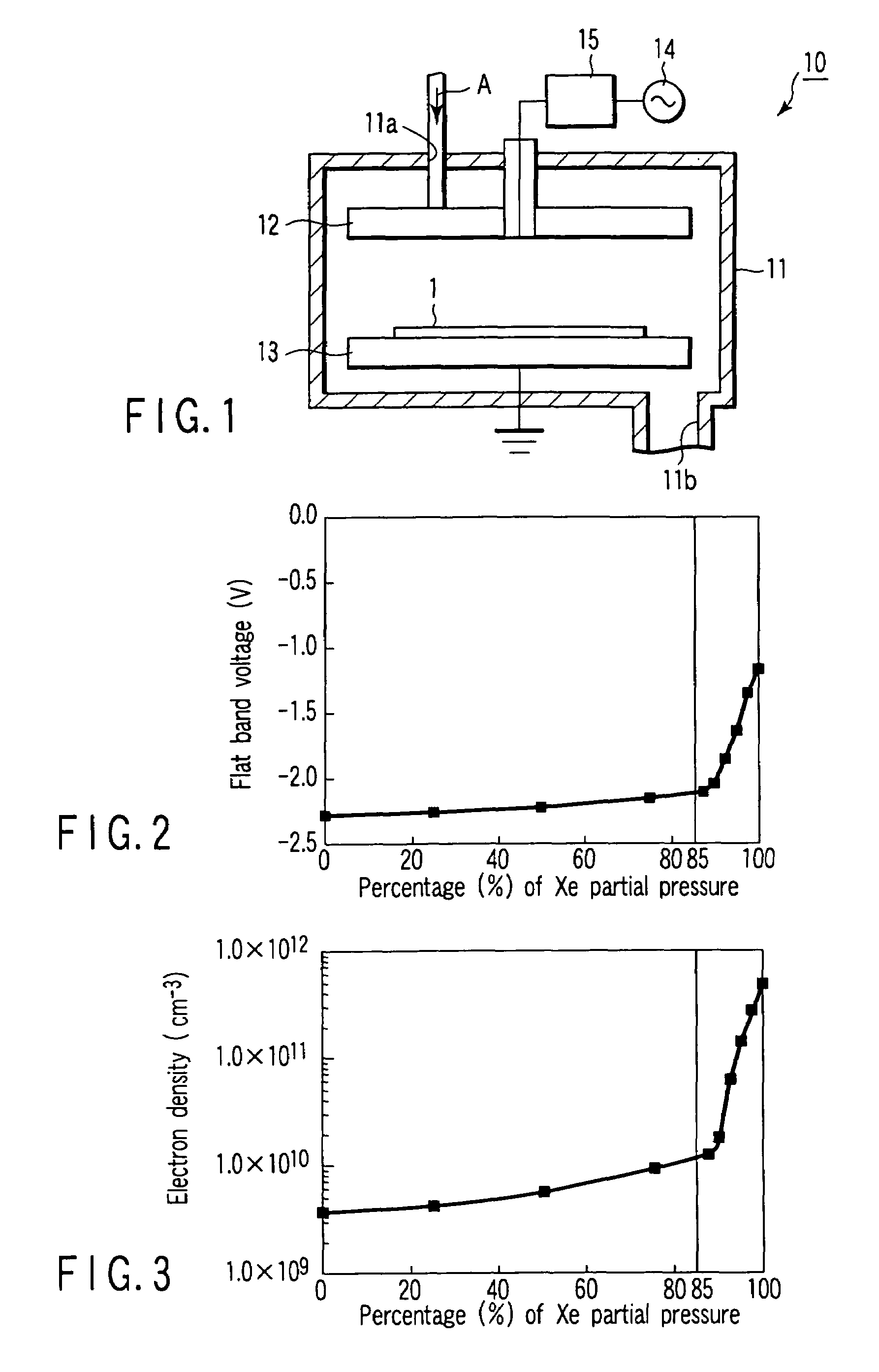
[0052]In the first step, a substrate 1 to be processed is prepared. The substrate 1 to be processed includes, for example, a silicon substrate for manufacturing a semiconductor device, a glass substrate for forming a display circuit of a liquid crystal display device, or a plastic substrate. In the first embodiment, the substrate to be processed is formed of, for example, a silicon substrate.

[0053]In the next step, prepared is a mixed gas consisting of at least three kinds of gases including a silicon compound gas formed of a compound having silicon (Si) atoms, an oxidizing gas, and a rare gas. Incidentally, it is possible to mix the silicon compound gas, the oxidizing gas and the rare gas in the process of introducing these gases into the chamber 1 so as to form the desired mixed gas.

[0054]In the first embodiment of the present invention, the mixed gas is prepared by mixing a tetraethoxy silane (Si(OCH2CH3)4: tetra ethyl ortho silicate) gas, i.e., TEOS gas, used as a silicon compou...

second embodiment

[0065]In the first embodiment described above, the gaseous pressure within the chamber 11 is set at 60 Pa. As a result, the percentage of the partial pressure of the TEOS gas based on the total pressure of the mixed gas is decreased with increase in the percentage of the partial pressure of the rare gas (Xe gas) based on the total pressure of the mixed gas, i.e., with increase in the degree of dilution with the rare gas. It follows that it is possible for the film-forming rate to be lowered depending on the percentage of the partial pressure of the rare gas (Pr) based on the total pressure of the mixed gas. Since the manufacturing time is one of the factors determining the manufacturing cost of the product, it is desirable for the film-forming time to be short. Such being the situation, a second embodiment of the present invention is directed to a film-forming method that permits improving the film-forming rate.

[0066]In the first step, a mixed gas is formed of gases including a sili...

third embodiment

[0076]In the first step, prepared is the substrate 1 to be processed. It is possible to use, for example, a silicon substrate for forming a semiconductor device, a glass substrate for forming the display circuit for a liquid crystal display device or a plastic substrate as the substrate 1 to be processed as in the first embodiment described previously. A silicon substrate is used in the third embodiment described in the following.

[0077]In the next step, prepared is a mixed gas consisting of at least three kinds of gases including a silicon compound gas, an oxidizing gas and a hydrogen gas (H2 gas). It is also possible to mix the silicon compound gas, the oxidizing gas and the hydrogen gas when these gases are introduced into the chamber 11 so as to form a desired mixed gas.

[0078]In the third embodiment of the present invention, the mixed gas is prepared by mixing a TEOS gas, which is used as a silicon compound gas and as an organometallic compound gas, an O2 gas used as an oxidizing...


PUM

PropertyMeasurementUnit
temperaturesaaaaaaaaaa
lengthaaaaaaaaaa
lengthaaaaaaaaaa

Abstract

Disclosed is a film-forming method, comprising supplying into a plasma processing chamber at least three kinds of gases including a silicon compound gas, an oxidizing gas, and a rare gas, the percentage of the partial pressure of the rare gas (Pr) based on the total pressure being not smaller than 85%, i.e., 85%≦Pr<100%, and generating a plasma within the plasma processing chamber so as to form a film of silicon oxide on a substrate to be processed.

Description

CROSS-REFERENCE TO RELATED APPLICATIONS[0001]This application is based upon and claims the benefit of priority from prior Japanese Patent Applications No. 2003-114640, filed Apr. 18, 2003; and No. 2004-095559, filed Mar. 29, 2004, the entire contents of both of which are incorporated herein by reference.BACKGROUND OF THE INVENTION[0002]1. Field of the Invention[0003]The present invention relates to a method of forming a film used in a semiconductor device such as a semiconductor integrated circuit device or a display device such as a liquid crystal display device. The present invention also relates to a method of manufacturing a semiconductor device such as a thin film transistor (TFT) or a metal oxide semiconductor device (MOS device) and to a semiconductor device. The present invention further relates to a method of manufacturing a display device such as a liquid crystal display device, an organic EL display device or an inorganic EL display device, and to a display device.[0004]2...

Claims


Application Information

Patent Timeline
Patent Type & Authority Patents(United States)
IPC IPC(8): H01L21/31C23C16/42C23C16/40G02F1/1368H01L21/205H01L21/316H01L21/768H01L29/786
CPCH01L21/31637H01L21/31641H01L21/31645H01L29/78696C23C16/401G02F1/1368H01L21/31616H01L21/02178H01L21/02181H01L21/02183H01L21/02189H01L21/02274H01L21/31608H01L21/02164
Inventor GOTO, MASASHIAZUMA, KAZUFUMINAKATA, YUKIHIKO
Owner ADVANCED LCD TECH DEVMENT CENT
Why Eureka
Eureka Blog
Learn More