
Structure and method for bonding to copper interconnect structures

a technology of interconnect structure and structure, applied in the direction of soldering apparatus, semiconductor/solid-state device details, manufacturing tools, etc., can solve the problems of not being implemented in commercial fabrication processes, unable to achieve the effect of reducing the number of holes, and increasing the difficulty of deposited conductive materials in the smaller openings

Active Publication Date: 2008-02-12
BELL SEMICON LLC
View PDF24 Cites 23 Cited by
  • Summary
  • Abstract
  • Description
  • Claims
  • Application Information

AI Technical Summary

Benefits of technology

[0026]The present invention comprises a method for forming a solder bond on a copper surface, comprising forming the copper surface, wherein unwanted copper oxide forms on the copper surface. The copper surface is reduced the copper oxide and the solder bond formed on the reduced copper surface.

Problems solved by technology

As integrated circuit devices and interconnect systems are reduced in size and made to carry higher frequency analog signals and higher data-rate digital signals, aluminum interconnect structures can impose unacceptable signal propagation delays within the chip.
Also, as via openings continue to shrink it becomes increasingly difficult to deposit conductive material in the smaller openings.
Although attempts have been made to wire bond to copper bond pads, these efforts remain an academic exercise and have not been implemented in commercial fabrication processes.
It is known that copper forms an oxide and corrodes when exposed to an ambient atmosphere.
Thus during shipment and storage at the packaging facility, exposed copper pads will oxidize.
Since the copper oxide continues to grow without limit, the oxide depth is unknown and any cleaning process employed to remove the copper oxide may not remove all of the oxide.
It is known that each mask layer can increase wafer cost and fabrication cycle time and lower the process yield.
Such intermetallic compounds may be brittle and susceptible to cracking, causing irregularities in the interface conductivity and degrading device performance.
Another mask step is required to form this aluminum layer, thus increasing the cost and process cycle time.
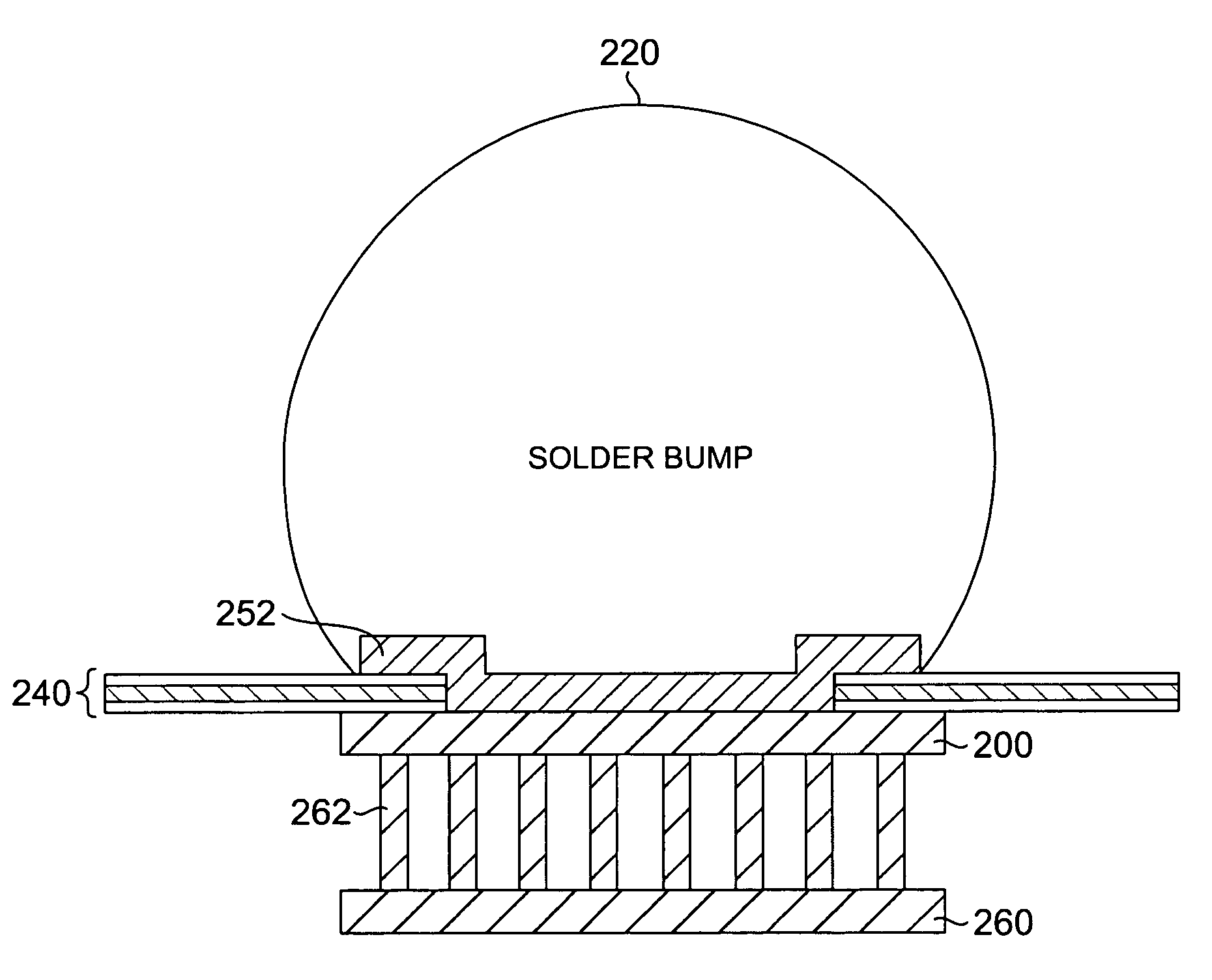
It is known that the conventional RF back-sputtering process (as described above in conjunction with the FIG. 6) for removing oxide (and other surface films) from the copper pad 200 can cause significant damage to the integrated circuit and the copper film surface.
Therefore, the device performance may be degraded when the RF back-sputtering process is used to clean the oxidized copper surface.
In the worst case, wafer plasma damage can occur, rendering the device useless.

Method used


Image

  • Structure and method for bonding to copper interconnect structures
  • Structure and method for bonding to copper interconnect structures
  • Structure and method for bonding to copper interconnect structures

Examples


Embodiment Construction

[0037]Before describing in detail the particular copper oxide cleaning process and a structure so formed in accordance with the present invention, it should be observed that the present invention resides primarily in a novel and non-obvious combination of elements and method steps. Accordingly, these elements and steps have been represented by conventional elements and steps in the drawings, showing only those specific details that are pertinent to the present invention so as not to obscure the description with structural details that will be readily apparent to those skilled in the art having the benefit of the description herein.

[0038]According to the teachings of the present invention, the prior art step of RF back-sputtering is replaced with a cleaning method that employs a reducing atmosphere to remove oxidation from a copper bond pad of an integrated circuit. In one embodiment the reducing atmosphere comprises a plasma containing hydrogen (H2) or ammonia (NH3) (or another hydr...


PUM

PropertyMeasurementUnit
lengthaaaaaaaaaa
lengthaaaaaaaaaa
surface reflectivityaaaaaaaaaa

Abstract

An integrated circuit structure and a method for fabricating the structure. The method comprises forming a copper bond pad for attaching the integrated circuit to a package. Copper oxide is removed from the pad by reduction in a hydrogen ion atmosphere. For attaching the integrated circuit to a bump-bonding package an under-bump metallization layer is formed over the reduced copper pad and a solder bump formed thereover. The process can also be employed in a wire bonding process by forming an aluminum layer overlying the cleaned copper pad. The structure of the present invention comprises a copper pad formed in a substrate. A passivation layer defining an opening therein overlies the copper pad. A under-bump metallization layer is disposed in the opening and a solder bump overlies the metallization layer. Alternatively, the structure further comprises an aluminum pad disposed overlying the reduced copper pad.

Description

[0001]This patent application claims the benefit of the provisional patent application filed on Dec. 20, 2002, and assigned application Ser. No. 60 / 435,033.BACKGROUND OF THE INVENTION[0002]Integrated circuits (or chips) comprise a silicon substrate and semiconductor devices, such as transistors, formed from doped regions within the substrate. A conductive interconnect system overlying the substrate electrically connects the doped regions to form electrical circuits.[0003]A conventional interconnect system comprises a plurality of substantially vertical conductive vias or plugs interconnecting one or more substantially horizontal conductive layers (each horizontal layer referred to as an “M” or metallization layer), with a dielectric layer disposed between two vertically adjacent conductive layers. A typical interconnect system comprises 6-9 horizontal conductive layers, each further comprising a plurality of conductive lines or traces. Conductive vias in the first or lowest intercon...

Claims


Application Information

Patent Timeline
Patent Type & Authority Patents(United States)
IPC IPC(8): B23K31/02B23K35/14H01L21/02H01L21/311H01L21/3213H01L21/60H01L23/485
CPCH01L21/02063H01L21/31116H01L21/32136H01L24/03H01L24/05H01L24/11H01L24/13H01L24/12H01L24/45H01L2224/0401H01L2224/05022H01L2224/05093H01L2224/05096H01L2224/05558H01L2224/05567H01L2224/05624H01L2224/05647H01L2224/11901H01L2224/13006H01L2224/13022H01L2224/13099H01L2224/45144H01L2224/48091H01L2224/48227H01L2224/48247H01L2224/48624H01L2224/48647H01L2224/8501H01L2924/01005H01L2924/01006H01L2924/01007H01L2924/01013H01L2924/01014H01L2924/01018H01L2924/01022H01L2924/01028H01L2924/01029H01L2924/01042H01L2924/01073H01L2924/01074H01L2924/01075H01L2924/01079H01L2924/01082H01L2924/01327H01L2924/014H01L2924/04941H01L2924/04953H01L2924/05042H01L2924/14H01L2924/15153H01L2924/15165H01L2924/01023H01L2924/01024H01L2924/01033H01L2224/05572H01L2224/131H01L2924/0001H01L2224/32225H01L2224/73265H01L2924/0002H01L2224/04042H01L2924/00014H01L2224/05552H01L2924/00H01L2224/05554H01L2224/49171H01L23/48
Inventor BACHMAN, MARK ADAMCHESIRE, DANIEL PATRICKMERCHANT, SAILESH MANSINH
Owner BELL SEMICON LLC
Learn More