

Charged particle beam apparatus
a particle beam and electron beam technology, applied in the field of scanning electron microscopes, can solve the problems of difficult to provide compact sem apparatus designed for stereoscopic observation, difficult to obtain high-resolution high-sensitivity image for observation, etc., and achieve the effect of high functionality
- Summary
- Abstract
- Description
- Claims
- Application Information
AI Technical Summary
Benefits of technology
Problems solved by technology
Method used
Image

Examples
first embodiment
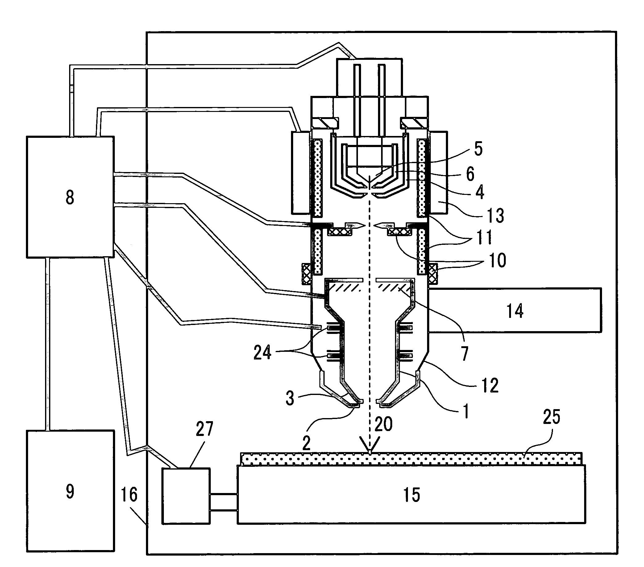
[0027]FIG. 1 schematically shows an embodiment of the present invention.
[0028]An electron source 5, such as a Schottky electron source, which is made of Zr / O / W, heated to 1600-1800 K, a suppressor electrode 6 and an extraction electrode 4 constitute an electron gun, which produces an electron beam probe 20 in the form of an electron beam. When the electron beam probe 20 impinges on a sample substrate 25, it is focused by an electrostatic objective lens, consisting of an objective lens inner electrode 3 located on the electron source side, and an objective lens sample side electrode 2 located on the sample side, so that it becomes a minute electron beam probe with a diameter of 30 nm to 2 nm. This beam is scanned in the x and y directions by a deflector 24, and released secondary electrons or backscattered electrons are detected by an electron detector 7 and converted into electrical signals, which signals are then processed by a controller 8, so that an SEM image appears on a displa...
second embodiment
[0055]FIG. 10 schematically shows a second embodiment of the present invention.
[0056]This embodiment concerns an inspection device for a mold 100 for use in the nano-in-print process as a means for formation of nanopatterns on substrates, to which the present invention is applied. The nano-in-print process is a process whereby nanopatterns are formed as follows: a thin coating of thermally or optically curable resin is formed on a Si, plastic or glass substrate; a mold is pressed against it to shape it; the resin is cured by heat or ultraviolet rays; then the mold is released. Because ultraviolet rays may be used and thermal expansion or plastic deformation is undesirable, the mold is made of glass or quartz. For this process, the 3D structure of the mold is important for the sake of mold releasability and pattern accuracy. The object size range for optical inspection, such as with a confocal microscope, is too small to measure this mold. On the other hand, the use of a conventional...
third embodiment
[0071]FIG. 13 shows an example of a focused ion beam system operating as a process unit, to which the present invention is applied. An ion beam probe 132, generated by an ion source 130, is focused by an electrostatic lens in an ion beam column 131 at an acceleration velocity of 10 to 30 kV, and it is cast on a sample substrate 25, whereby a desired area is cut by ion beam etching. In this system, an SEM column 101 according to the present invention, which is tilted at an angle ω, can be moved by transport means 14 to vary the working distance WD. When the working distance WD is between 5 mm and 10 mm, a wider area can be observed though the resolution is low, and staining due to sample element redeposition is reduced. Therefore, the SEM is used as a monitor during radiation of an ion beam and to detect an end point. It is also used to get an overall view of a sample area. On the other hand, when the working distance WD is shorter, specifically between 1 mm and 5 mm, observation wit...
PUM
 Abstract
Description
Claims
Application Information