Feedback circuit for output control in a semiconductor X-ray detector

a technology of output control and x-ray detector, which is applied in the field of x-ray detectors, can solve the problems of not being able to accommodate x-ray photon counts, requiring cryogenic temperatures for greatest accuracy, and difficulty in interpreting their significan

Active Publication Date: 2008-03-04
THERMO ELECTRONICS SCI INSTR LLC
View PDF2 Cites 28 Cited by
  • Summary
  • Abstract
  • Description
  • Claims
  • Application Information

AI Technical Summary

Benefits of technology

[0009]A voltage-controlled resistance 104 is then provided, and has an input terminal 106 (connected in communication with the semiconductor detector 102), an output terminal 108, and a control voltage supply terminal 110, wherein the output terminal 108 is biased by the control voltage terminal 110 (which is preferably supplied with an at least substantially constant voltage Supply VDD) to have a voltage at least substantially proportional to the voltage at the input terminal 106. The voltage-controlled resistance 104 preferably takes the form of a field effect transistor (FET) operating in its ohmic / triode range, with gate 106, source 108, and drain 110, and thus the remainder of this discussion will assume a FET is used as the resistance 104. A current source 112 is usefully provided to assist in biasing the FET 104 at the gate 106. As a result of this arrangement, the voltage at the source / output terminal 108 varies in accordance with the time and energy of the X-ray photons 14 incident on the semiconductor detector 102.

Problems solved by technology

While this arrangement worked well, it disadvantageously had a response which is rather slow by present standards—it could not accommodate X-ray photon counts of greater than approximately 60,000 counts per second—and additionally it required cooling to cryogenic temperatures for greatest accuracy.
Unfortunately, SDD's carry their own drawbacks, in particular the problem of varying detector response with x-ray illumination level: the SDDs, which often have an integrated FET provided for signal amplification purposes, have a gain which changes with voltage (Hansen et al., Dynamic Behavior of the Charge-to-Voltage Conversion in Si-Drift Detectors With Integrated JFETs, IEEE Transactions On Nuclear Science, Vol. 50, No. 5, October 2003).
This results in variations in the measurements of detected X-rays, and in turn difficulties in interpreting their significance.
As noted by Fiorini, feedback to the drain can help reduce peak shift (shift in the peak on an intensity / counts vs. measured energy scale), it does not solve the problem of resolution degradation.

Method used


Image

  • Feedback circuit for output control in a semiconductor X-ray detector
  • Feedback circuit for output control in a semiconductor X-ray detector
  • Feedback circuit for output control in a semiconductor X-ray detector

Examples


Embodiment Construction

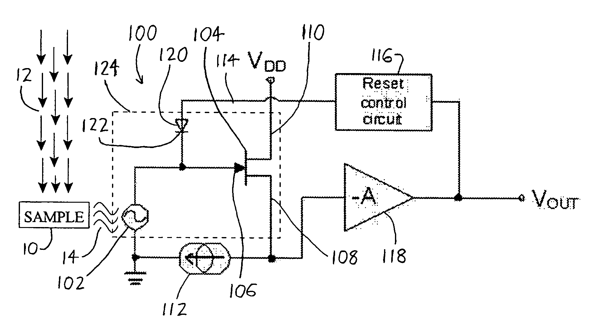
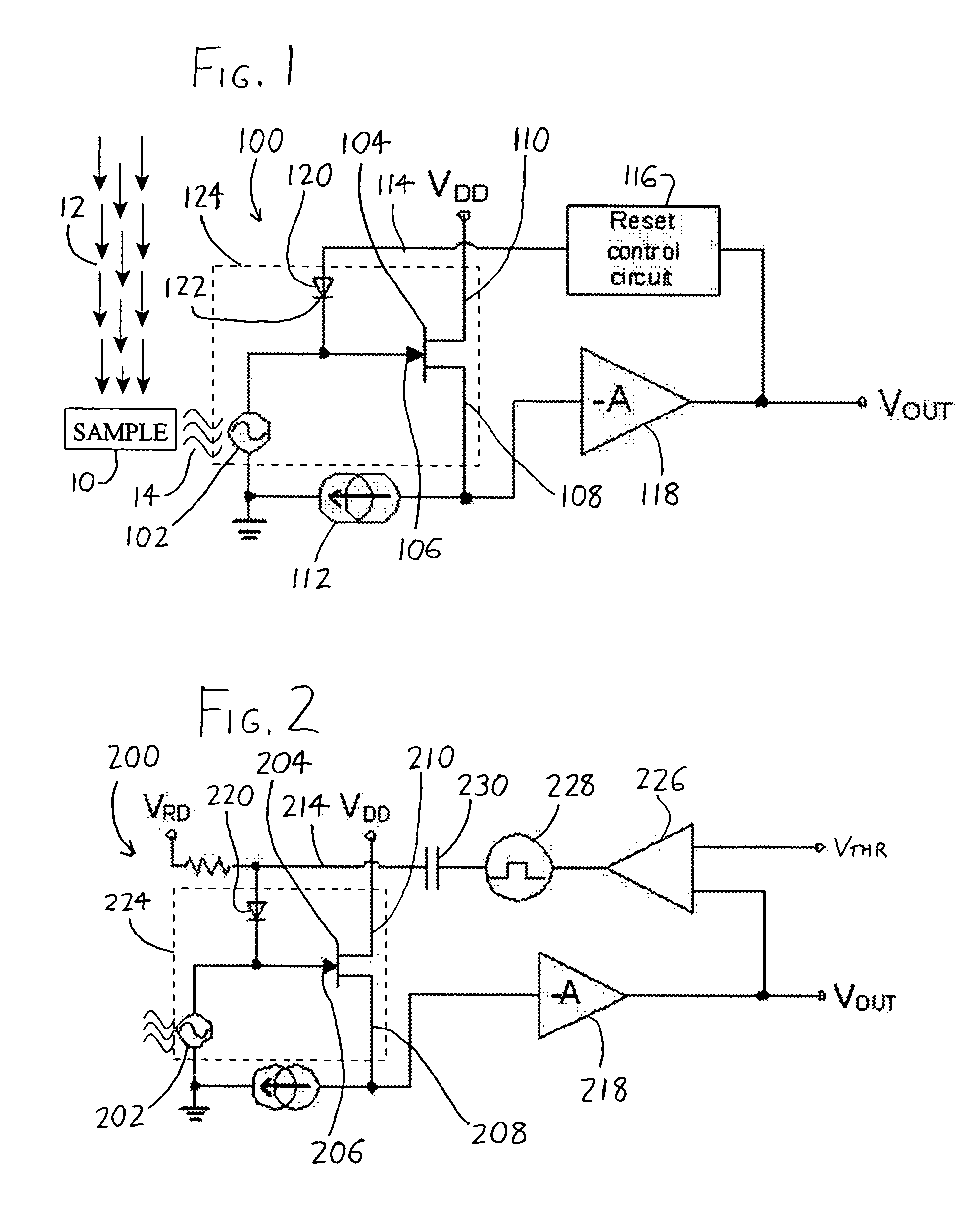
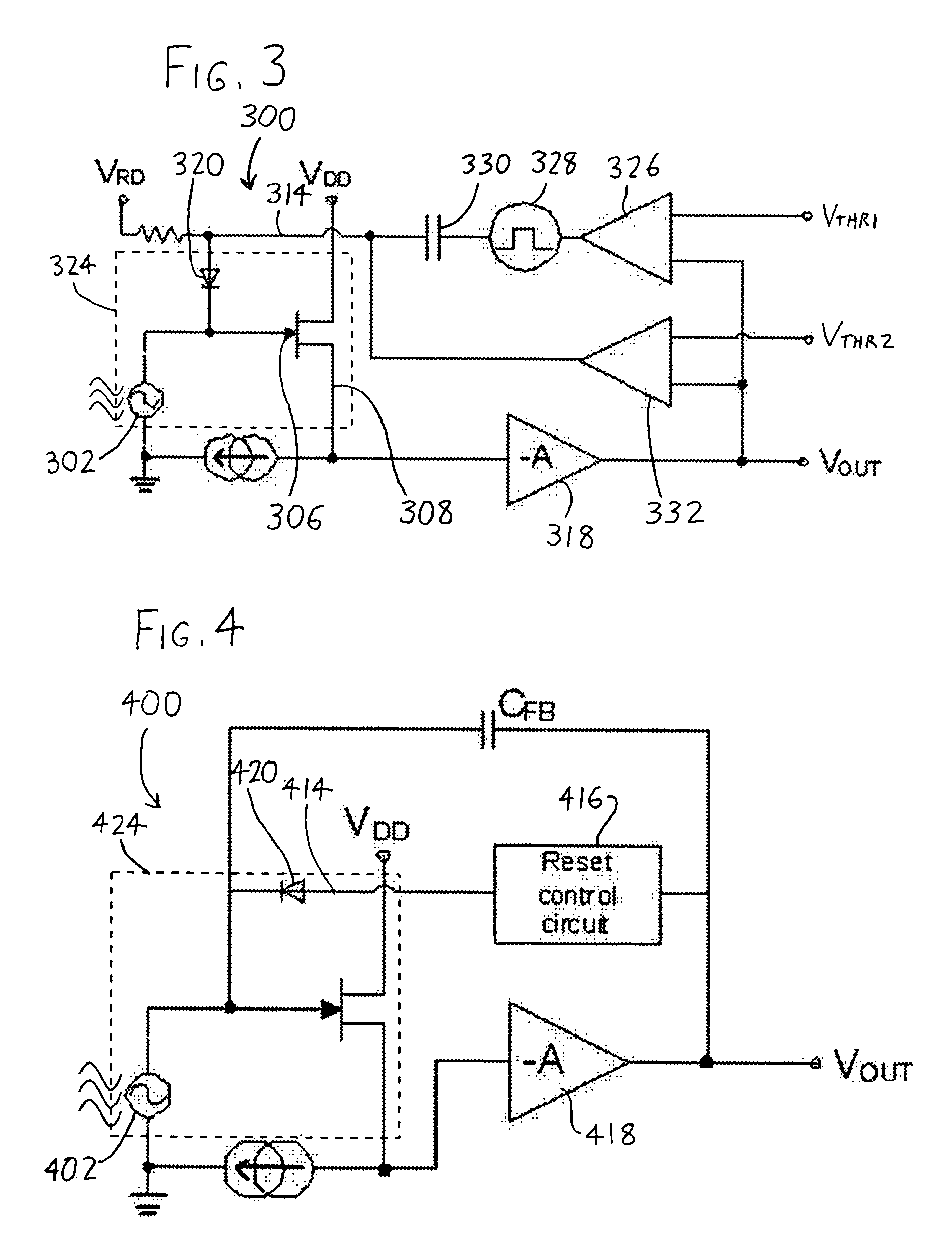
[0019]Following is a list of exemplary components that may be used in the foregoing detectors, though it should be understood that any other suitable components may be used.

[0020]The semiconductor detectors 102 / 202 / 302 / 402 (and more generally the detector chips / blocks 124 / 224 / 324 / 424) may take the form of PSD-10-130, PSD-30-140, or SD3-10-128 Silicon Drift Detector modules from PNSensor GmbH (Munich, Germany), which usefully have an onboard FET.

[0021]The amplifiers / buffers 118 / 218 / 318 may take the form of the AD829 operational amplifier (Analog Devices, Norwood, Mass., USA) operating in net unity gain. However, this is not preferred for the amplifier 418, which has nonunity gain for optimal operation. Thus, the amplifiers 118 / 218 / 318 / 418 may take the form of a two-stage amplifier using the foregoing AD829 operational amplifier, e.g., with the first stage amplifier providing a non-inverting voltage gain of 16, and the second stage amplifier providing an inverting voltage gain of 4 (a...


PUM


Abstract

An X-ray detector using a semiconductor detector, most preferably a Silicon Drift Detector, utilizes a field effect transistor or other voltage-controlled resistance to generate an output voltage proportional to its input charge (which is generated by the X-ray photons incident on the semiconductor detector). To keep the charge (and thus the output voltage) to an acceptable range—one wherein the relationship between output voltage and input charge is substantially proportional—a feedback circuit is provided between the output and input terminals, wherein the charge on the input terminal is depleted when the output voltage begins leaving the desired range. Preferably, this is done by a comparator which monitors the output voltage, and provides a reset signal to the input terminal when it begins moving out of range. Alternatively or additionally, the reset signal may be a pulse supplied to the input terminal from a pulse generator activated by the comparator.

Description

FIELD OF THE INVENTION[0001]This document concerns an invention relating generally to X-ray detectors, and more specifically to X-ray detectors used in microanalysis and X-ray fluorescence measurement (e.g., in electron microscopes and X-ray spectrometers).BACKGROUND OF THE INVENTION[0002]X-ray detectors are used in electron microscopes (e.g., scanning electron microscopes and tunneling electron microscopes), X-ray spectrometers (e.g., X-ray fluorescence spectrometers / energy-dispersive X-ray spectrometers), and other instruments to analyze the composition and properties of materials. An illumination source (such as an electron beam or X-ray source) is directed at a sample to be analyzed, resulting in emission of X-rays from the sample wherein the X-rays (X-ray photons) have energies which are characteristic of the atoms of the sample from which they were emitted. Thus, the counts and energies of the emitted X-rays can indicate the composition of the sample.[0003]Traditionally, X-ray...

Claims


Application Information

Patent Timeline
Patent Type & Authority Patents(United States)
IPC IPC(8): G01T1/24
CPCG01T1/2928
Inventor DRUMMOND, WILLIAM E.FAHRBACH, DAVID R.HOWARD, JAMES V.MISENHEIMER, MARK E.STOCKER, DEAN A.
Owner THERMO ELECTRONICS SCI INSTR LLC
Why Eureka
Try Eureka