
Copper foil having blackened surface or layer
a technology of blackened surface and copper foil, applied in the field of copper foil with a blackened surface or layer, can solve the problems of deterioration of optical transmission, inferior screen contrast, and generation of electromagnetic waves such as microwaves and infrasonic waves, and achieve superior shielding characteristics, effective shielding, and superior
- Summary
- Abstract
- Description
- Claims
- Application Information
AI Technical Summary
Benefits of technology
Problems solved by technology
Method used
Image

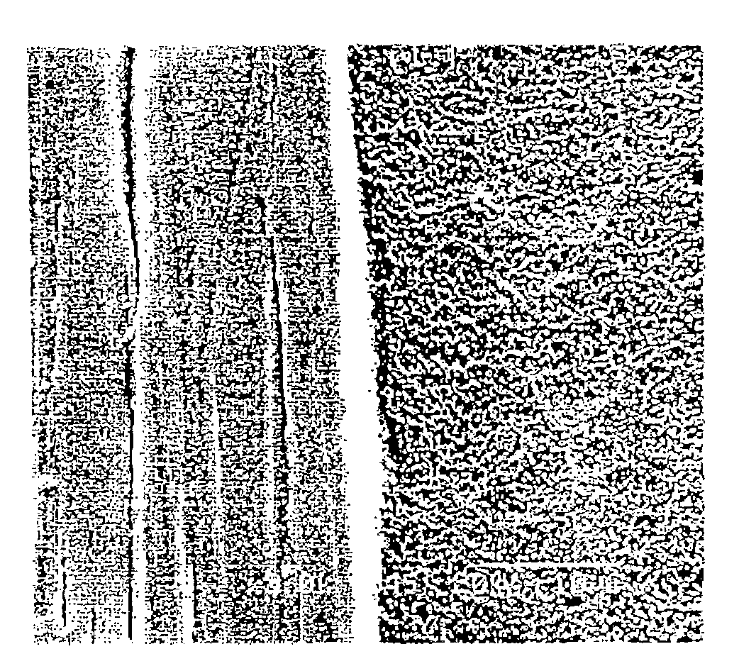
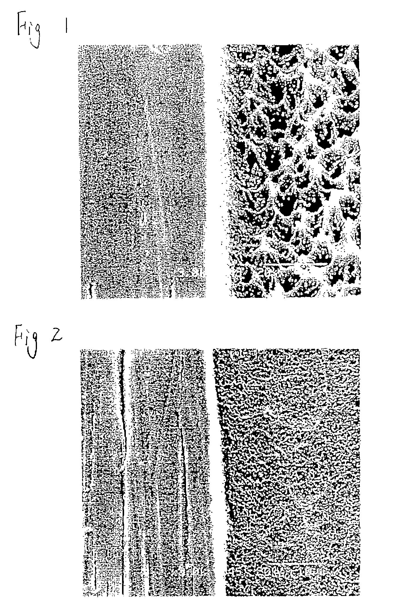
Examples
examples
[0097]Examples of the present invention are now explained. These Examples merely illustrate a preferred example, and the present invention shall in no way be limited thereby. In other words, all modifications, other embodiments and modes covered by the technical spirit of the present invention shall be included in this invention.
[0098]Incidentally, the Comparative Examples are indicated in the latter part for comparison with the present invention.
examples 1 to 28
[0099]An electrolytic copper foil or rolled copper foil having a thickness of 9, 12 and 18 μm was degreased, water washed, pickled and water washed, and a black plated layer was formed using the various types of plating baths described above. The plating conditions are shown in Table 1.
[0100]For degreasing, a standard alkali degreasing fluid GN cleaner 87: 30 g / L was used, and electrolytic degreasing was performed using a stainless anode at 15 A / dm2, for 5 seconds, at 40° C. Further, pickling was performed for 10 seconds at room temperature with H2SO4: 100 g / L.
[0101]
TABLE 1PlatingCoat PlatingFoil ThicknessCurrent DensityTimeSolutionSolutionSolutionCopper Foil(μm)(A / dm2)(sec)Temperature (° C.)PHExample 1Cu—Ni—(1) M Surface18401.5402.5Example 2Cu—Ni—(1) M Surface12401.5402.5Example 3Cu—Ni—(1) M Surface9352.2402.5Example 4Cu—NiNi—Co(2) M Surface18401.5402.5Example 5Cu—NiNi—Co(2) M Surface12401.5402.5Example 6Cu—NiNi—Co(2) M Surface9352.2402.5Example 7Cu—Ni—(2) S Surface12451.5402.5Exam...
PUM
| Property | Measurement | Unit |
|---|---|---|
| surface roughness Ra | aaaaa | aaaaa |
| surface roughness Ra | aaaaa | aaaaa |
| surface roughness Ra | aaaaa | aaaaa |
Abstract
Description
Claims
Application Information