

Semiconductor device and method for high-k gate dielectrics
a semiconductor device and dielectric technology, applied in the direction of semiconductor devices, electrical equipment, transistors, etc., can solve the problems of bias temperature instability, increased gate-to-channel leakage current, and fabrication problems associated with forming gate dielectric layers that include high-k materials
- Summary
- Abstract
- Description
- Claims
- Application Information
AI Technical Summary
Benefits of technology
Problems solved by technology
Method used
Image

Examples
Embodiment Construction
[0020]The operation and fabrication of the presently preferred embodiments are discussed in detail below. However, the embodiments and examples described herein are not the only applications or uses contemplated for the invention. The specific embodiments discussed are merely illustrative of specific ways to make and use the invention, and do not limit the scope of the invention or the appended claims.
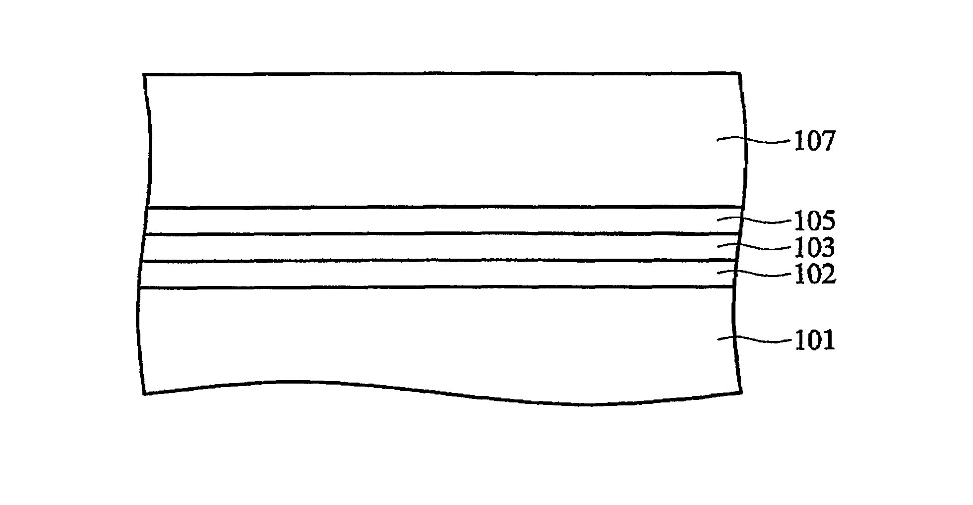
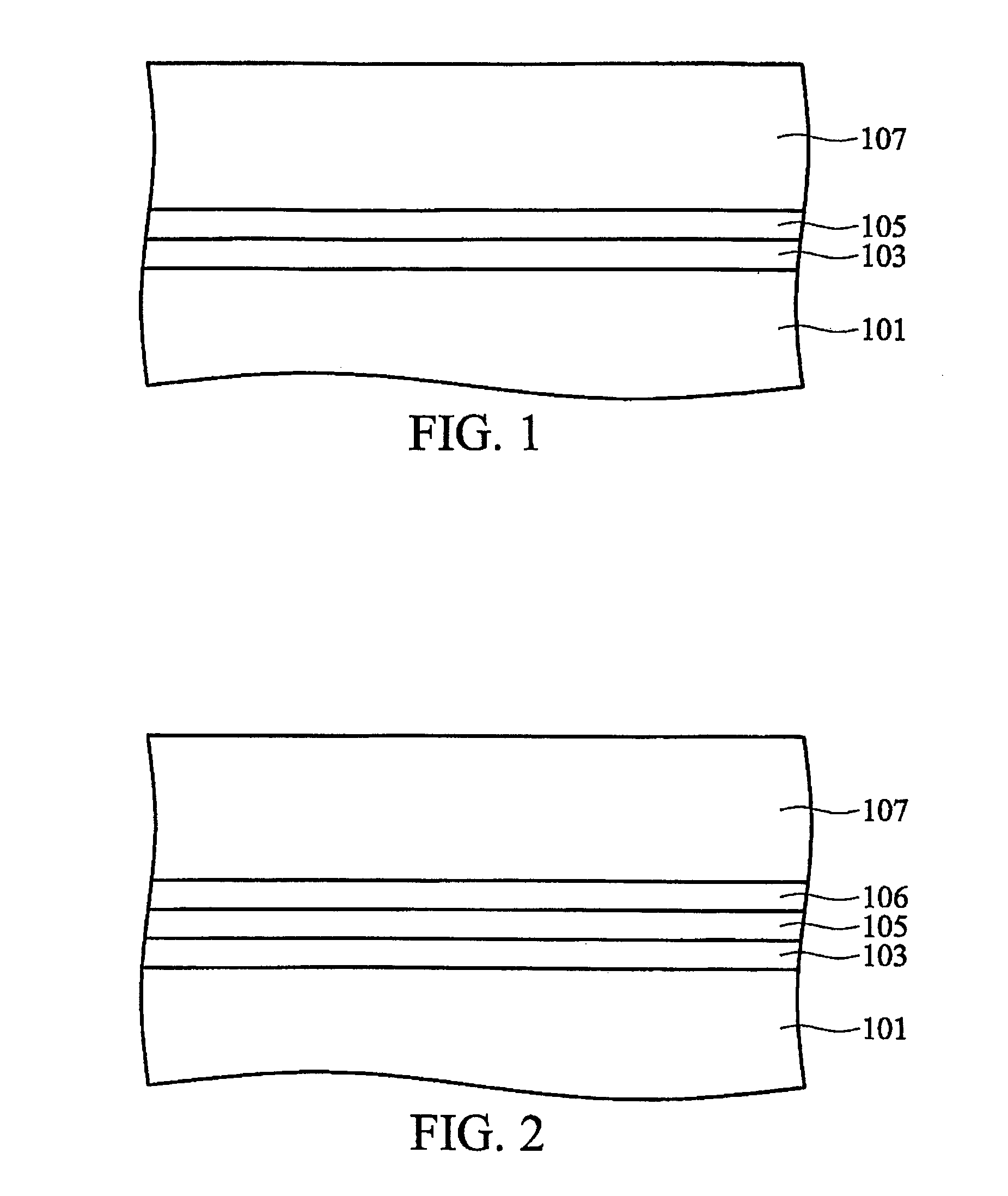
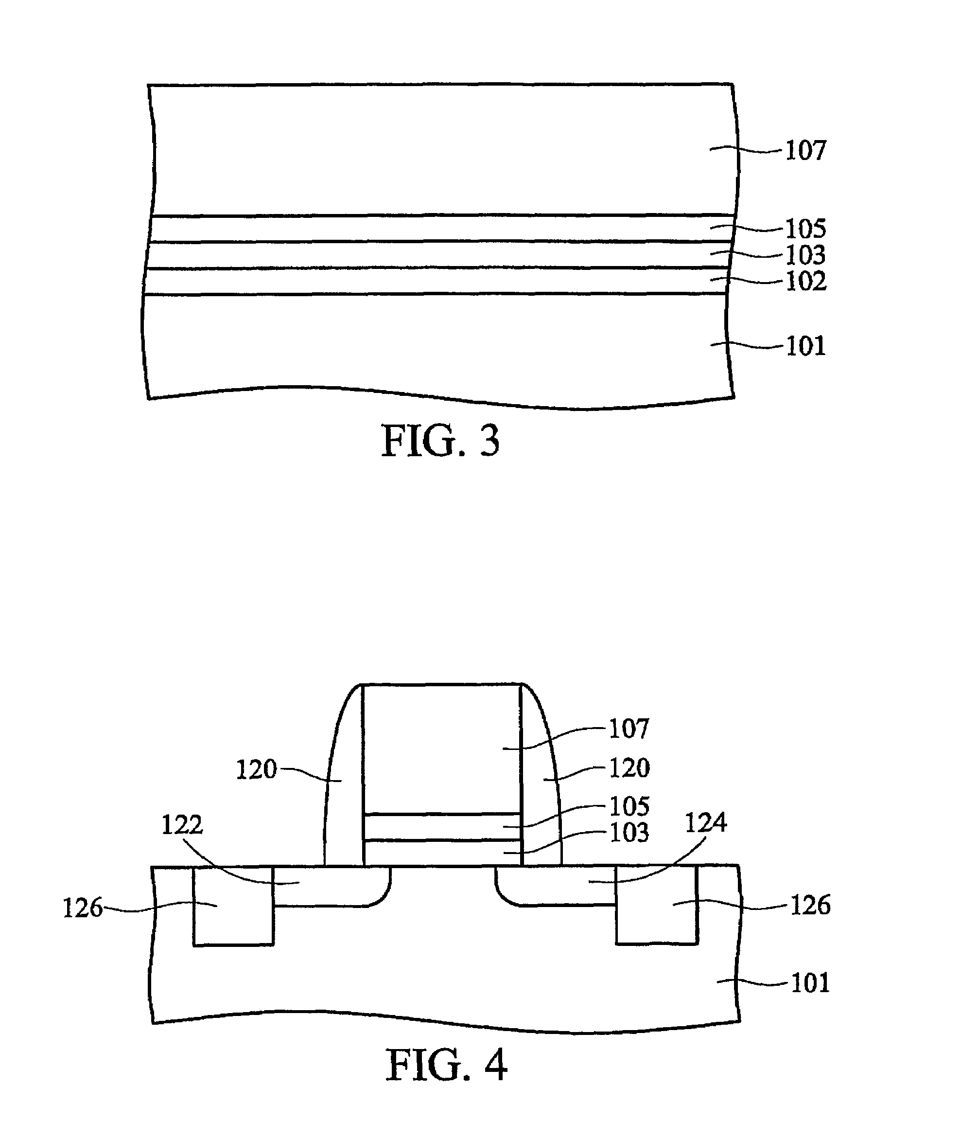
[0021]FIG. 1 depicts a cross sectional view of an integrated circuit at an intermediate fabrication stage. It is not drawn to scale, but drawn as an illustration only. A semiconductor substrate 101 is preferably a silicon wafer, however, the substrate 101 may alternatively comprise Ge, SiGe, strained silicon, strained germanium, GaAs, silicon on insulator (SOI), germanium on insulator (GOI), a combination, or a stacked arrangement of layers such as Si / SiGe.
[0022]Preferably, a first nitrogen-containing layer 103 is deposited using conventional jet vapor deposition (JVD). In preferred em...
PUM
| Property | Measurement | Unit |
|---|---|---|
| thick | aaaaa | aaaaa |
| thick | aaaaa | aaaaa |
| dielectric constant | aaaaa | aaaaa |
Abstract
Description
Claims
Application Information