Laser-based irradiation apparatus and method to measure the functional dose-rate response of semiconductor devices

a laser-based irradiation and functional technology, applied in the direction of optical radiation measurement, instruments, material analysis, etc., can solve the problems of devices becoming even more sensitive to transient ionizing radiation effects, known deleterious effects on semiconductor devices and circuits, and degrading the performance of electronic devices

Active Publication Date: 2008-05-20
NAT TECH & ENG SOLUTIONS OF SANDIA LLC
View PDF4 Cites 9 Cited by
  • Summary
  • Abstract
  • Description
  • Claims
  • Application Information

AI Technical Summary

Benefits of technology

[0010]The present invention is directed to a broad-beam laser irradiation apparatus for measuring the dose-rate response of a semiconductor device under test (DUT), comprising at least one infrared laser that produces a broad-area pulse of laser light, having a laser pulsewidth and intensity, directed onto the surface of the semiconductor device, and means for measuring the dose-rate response resulting from the laser irradiation of the surface of the semiconductor device. The infrared laser can be a laser diode. The apparatus can further comprise means for varying the pulsewidth and intensity of the laser pulse. The apparatus can further comprise an imaging device to image the laser irradiation and an energy detector to measure the energy of the laser irradiation of the surface of the semiconductor device. One or more beam splitters can be used to simultaneously measure the energy transmitted to the device from the one or more laser sources. The broad-beam laser irradiation apparatus can be used for non-destructive, bench-top, dose-rate equivalent testing of semiconductor devices, and in a specific application, can determine if aging has affected the device's overall functionality. Further, for devices exposed to dynamically changing radiation environments, the apparatus can replicate the time-varying, dose-rate intensity of a space, high altitude, or hostile military environment.

Problems solved by technology

The effects of harsh radiation environments, such as are encountered in space, military, or nuclear power applications, are known to have deleterious effects on semiconductor devices and circuits.
Recent studies have further shown that prolonged exposures to even low levels of radiation can degrade the performance of electronic devices.
Compounding these effects, the continued reduction in feature size of modern commercial integrated circuits (ICs) can result in these devices becoming even more sensitive to transient ionizing radiation effects.
The generation and collection of this unintended electrical charge within the circuit can alter the performance and reliability of specific circuit structures within the device.
Historically, the greatest obstacle to measure the radiation response of electronic devices used in long-lived electrical systems has been the destructive nature of most traditional radiation testing techniques.
Indeed, such exposures reproduce many bulk material radiation effects (e.g., shock, thermal effects, and secondary radiations) that the laser cannot.
However, in the context of photocurrent collection and circuit electrical operation, the additional energy deposition deep in the sample only produces electron-hole pairs that may contribute to thermal and mechanical effects, but not to electrical behavior.

Method used


Image

  • Laser-based irradiation apparatus and method to measure the functional dose-rate response of semiconductor devices
  • Laser-based irradiation apparatus and method to measure the functional dose-rate response of semiconductor devices
  • Laser-based irradiation apparatus and method to measure the functional dose-rate response of semiconductor devices

Examples


embodiment 30

[0038]Using beam splitters, the laser pulse energy, laser beam uniformity, and the position of the semiconductor device within the exposure area of the laser beam can be simultaneously measured during each exposure of a sequence of exposures. In FIG. 5A is shown an embodiment 30 in which a beam splitter 31 is employed to transmit a fixed fraction 33 of the incident laser beam 32 toward the DUT 22, while the remainder 34 of the beam 32 is reflected onto the energy detector 25. The beam splitter 31 is selected so as to: (1) match the wavelength of the laser light source, (2) accommodate the heat loads from energy deposition in the beam splitter by the laser pulses, (3) accommodate the lateral size of the laser beam, and (4) provide the desired fractional split between transmission 33 and reflection 34 of the incident laser beam 32. For the examples presented herein, a 50-50 beam splitter was used (i.e. 50% of the incident beam is transmitted straight through the beam splitter and 50% ...

embodiment 20

[0048]The electrical response of a DUT can be measured for one or more laser light exposures and compared to a specified value to determine a deposited energy dependence of the failure of the semiconductor device. In FIG. 9 are shown results of a typical laser dose-rate logic failure test of four different logic inverter circuits (i.e., Devices A, B, C, and D) measured with the embodiment 20 shown in FIG. 3A. Failure in the devices is seen to occur when the minimum inverter output voltage falls below the manufacturer-specified value of Voh=2.7V at 400 μA. In this example, the failure is determined to be caused by a total energy deposition of about 12 μJ, corresponding to an equivalent dose-rate of about 108 rad(Si) / s.

[0049]The broad-beam laser irradiation apparatus can be used to control the time-duration of the incident radiation pulse, varying from hundreds of nanoseconds to DC exposures. This time-duration feature can be used to examine the dependence of a device's failure on the...
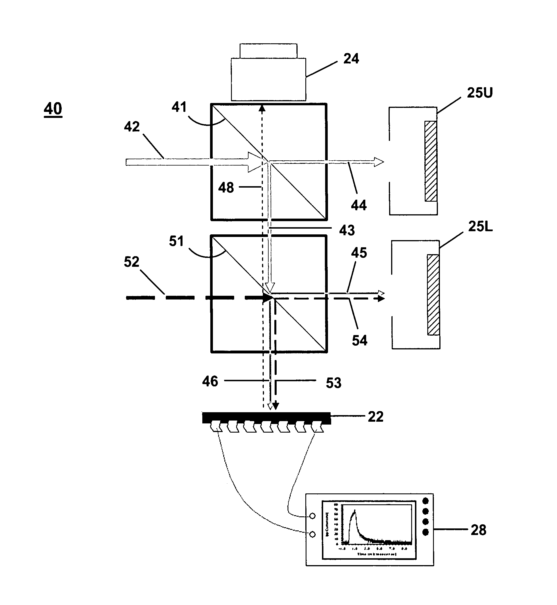
embodiment 40

[0051]The injection current of the laser diode arrays can also be modulated to produce a time-varying, intensity-varying dose-rate equivalent laser exposure, within the dynamic limits of the single laser diode or diode array. Alternatively, embodiment 40 enables the use of multiple lasers, fired in a synchronized sequence, to deliver a greater range of laser intensities than is possible with any single laser diode array. This, in turn, can be used in conjunction with the injection of a pre-characterized, controlled, external, electrical transient on the power and ground lines of the DUT, whose introduction is synchronized with the delivery of the laser pulse. This combination of stimuli to the DUT replicates the charge generation effects of the dose-rate exposure internal to the DUT and the external electrical transients that the DUT experiences from the surrounding circuit's exposure to the radiation.

[0052]Thus, the broad-beam laser irradiation apparatus can be used to recreate a t...


PUM


Abstract

A broad-beam laser irradiation apparatus can measure the parametric or functional response of a semiconductor device to exposure to dose-rate equivalent infrared laser light. Comparisons of dose-rate response from before, during, and after accelerated aging of a device, or from periodic sampling of devices from fielded operational systems can determine if aging has affected the device's overall functionality. The dependence of these changes on equivalent dose-rate pulse intensity and / or duration can be measured with the apparatus. The synchronized introduction of external electrical transients into the device under test can be used to simulate the electrical effects of the surrounding circuitry's response to a radiation exposure while exposing the device to dose-rate equivalent infrared laser light.

Description

CROSS-REFERENCE TO RELATED APPLICATIONS[0001]This application is a continuation-in-part of U.S. patent application Ser. No. 11 / 315,676, filed Dec. 22, 2005, now abandoned which is a continuation-in-part of U.S. patent application Ser. No. 10 / 810,420, filed Mar. 25, 2004, now U.S. Pat. No. 7,019,311, which are both incorporated herein by reference.STATEMENT OF GOVERNMENT INTEREST[0002]This invention was made with Government support under contract no. DE-AC04-94AL85000 awarded by the U.S. Department of Energy to Sandia Corporation. The Government has certain rights in the invention.FIELD OF THE INVENTION[0003]The present invention relates to ionizing radiation effects in semiconductor devices and, in particular, to a laser-based irradiation apparatus and method to measure the functional and parametric response of semiconductor devices to pulsed laser irradiation.BACKGROUND OF THE INVENTION[0004]The effects of harsh radiation environments, such as are encountered in space, military, or...

Claims


Application Information

Patent Timeline
Patent Type & Authority Patents(United States)
IPC IPC(8): G01R31/00
CPCG01R31/2881G01R31/311
Inventor HORN, KEVIN M.
Owner NAT TECH & ENG SOLUTIONS OF SANDIA LLC
Why Eureka
Try Eureka