Electron-emitting device, electron source, image display device and information display and reproduction apparatus using image display device, and method of manufacturing the same

a technology of image display device and electron emission device, which is applied in the manufacture of electric discharge tube/lamp, discharge tube luminescnet screen, discharge tube/light tube, etc., can solve the problems of abnormal discharge, deterioration of electron emission characteristics of electron-emitting device, and potential on the insulating surface, so as to achieve stable electron emission characteristics and more stable electron emission characteristics

Inactive Publication Date: 2008-06-24
CANON KK
View PDF19 Cites 11 Cited by
  • Summary
  • Abstract
  • Description
  • Claims
  • Application Information

AI Technical Summary

Benefits of technology

[0013]The present invention has been devised in order to solve or alleviate the problems, and it is an object of the invention to provide an electron-emitting device in which abnormal discharge near the electron-emitting device is avoided and electron emission characteristics are stable and a method of manufacturing the electron-emitting device. It is another object of the invention to provide an electron source and an image display device, an information display and a reproduction apparatus, which use the electron-emitting device, and a method of manufacturing the same.
[0025]As described above, the electron-emitting device of the invention is a lateral type FE electron-emitting device in which the resistive film is provided between the cathode electrode and the gate electrode as a film for suppressing charging. Thus, it is possible to suppress charged particles (such as electrons and ions) from being injected into the surface of the insulating substrate to generate secondary electrons and cause abnormal discharge under a high electric field and marked fall in electron emission characteristics of the electron-emitting device. In addition, since the end portion (the side surface) of the cathode electrode opposed to the gate electrode is also covered with the resistive film, it is possible to create a situation where electrons to be injected into the surface of the insulating substrate between the cathode electrode and the gate electrode are not emitted. Therefore, it is possible to obtain an electron-emitting device in which the abnormal discharge is less likely to occur and the electron emission characteristics are more stable.
[0026]When the electron-emitting device manufactured by the manufacturing method of the invention is applied to an electron source and an image display device, it is possible to realize an electron source and an image display device in which the abnormal discharge is less likely to occur and the electron emission characteristics are stable.

Problems solved by technology

As a cause of instability of electron emission characteristics of the electron-emitting devices, there is instability of a potential on a surface of an insulating surface of the first substrate located near an electron-emitting region, which is caused by exposure of the insulating surface.
The instability of a potential on the insulating surface is caused because a potential, due to capacity depending on a dielectric constant of an insulator and a vacuum, is generated on the insulating surface around the electron-emitting devices by a high voltage of 1 kV to 30 kV applied to the anode electrode.
The generation of the secondary electrons results in abnormal discharge particularly under a high electric field.
Thus, the electron emission characteristics of the electron-emitting devices deteriorate markedly and, in the worst case, the electron-emitting devices are destroyed.
However, it is conceivable that the abnormal discharge is caused by charging of the insulating surface due to injection of charged particles (such as electrons emitted from the electron-emitting devices and ions generated by the emitted electrons) into the insulating substrate or by avalanche effect of electrons due to emission of secondary electrons from the charged insulating surface.

Method used


Image

  • Electron-emitting device, electron source, image display device and information display and reproduction apparatus using image display device, and method of manufacturing the same
  • Electron-emitting device, electron source, image display device and information display and reproduction apparatus using image display device, and method of manufacturing the same
  • Electron-emitting device, electron source, image display device and information display and reproduction apparatus using image display device, and method of manufacturing the same

Examples


embodiments

[0095]Embodiments according to this embodiment mode will be hereinafter explained in detail.

first embodiment

[0096]A method of manufacturing an electron-emitting device of this embodiment will be hereinafter explained in detail with reference to FIGS. 10A to 10G.

(Step 1)

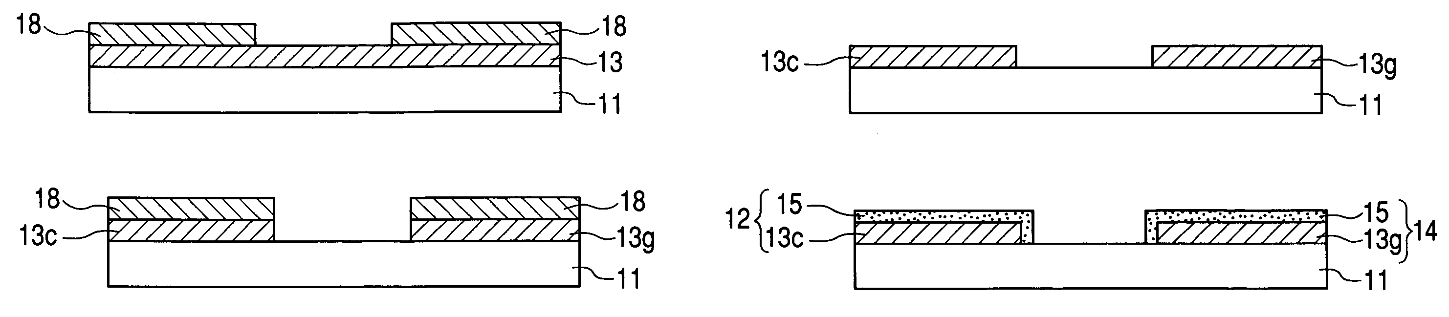
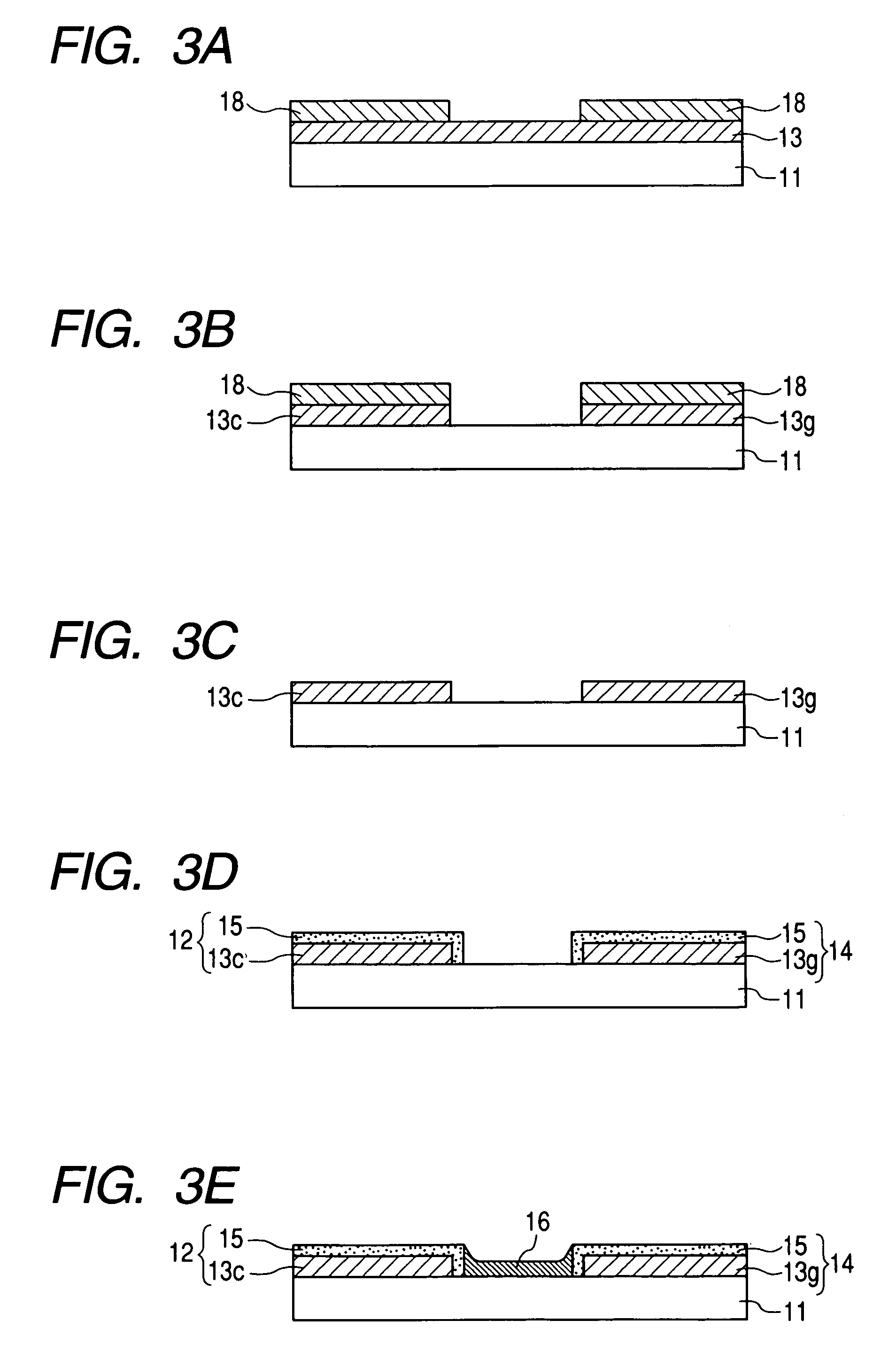
[0097]First, as shown in FIG. 10A, a quartz glass was used for the substrate 11 and, after sufficiently cleaning the substrate 11, W with a thickness of 100 nm was deposited on the substrate 11 as the conductive layer 13 by the sputtering method. Subsequently, a positive photoresist was spin-coated on the conductive layer 13 and a photo-mask pattern was exposed and developed to form the mask pattern 18.

[0098]The mask pattern 18 was formed excluding a portion to be dry-etched in order to form the cathode electrode 13c and the gate electrode 13g in the next step. Here, an opening width of the mask pattern 18 was set to 5 μm.

(Step 2)

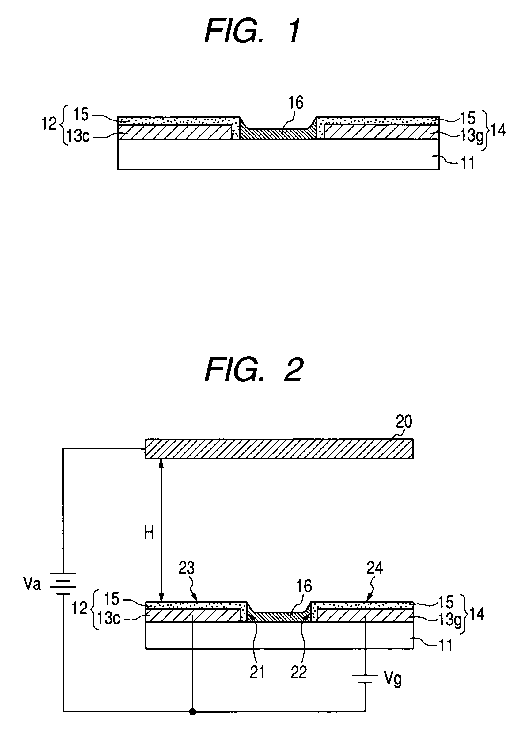
[0099]Next, as shown in FIG. 10B, the conductive layer 13 was pierced through by dry etching to separate the conductive layer 13 into two (form a space) and form the cathode electrode 13c and the g...

second embodiment

[0109]FIGS. 11A to 11F are schematic sectional views showing steps of manufacturing the electron-emitting device of this embodiment. In this embodiment, the resistive film 16 was formed by the printing method of the ink jet system. Here, only characteristic parts of this embodiment will be explained, and explanations repeating the explanations of the first embodiment will be omitted.

(Step 1)

[0110]First, as shown in FIG. 11A, a quartz glass was used for the substrate 11 and, after sufficiently cleaning the substrate 11, W with a thickness of 100 nm was deposited on the substrate 11 as the conductive layer 13 by the sputtering method. Subsequently, a positive photoresist was spin-coated on the conductive layer 13 and a photo-mask pattern was exposed and developed to form the mask pattern 18. The mask pattern 18 was formed excluding a portion to be dry-etched in order to form the cathode electrode 13c and the gate electrode 13g in the next step. Here, an opening width of the mask patte...


PUM


Abstract

The present invention provide a lateral type electron-emitting device in which abnormal discharge near an electron-emitting region is suppressed, electron emission characteristics are stable, and electron emission efficiency is high. A method of manufacturing an electron-emitting device of the invention includes: a first step of preparing an electron-emitting electrode and a control electrode that are arranged on a surface of an insulating substrate; and a second step of covering the surface of the insulating substrate, which is located between the electron-emitting electrode and the control electrode, with a resistive film to connect the electron-emitting electrode and the control electrode. In the method of manufacturing an electron-emitting device, the resistive film is arranged to cover an end of a surface of the electron-emitting electrode opposed to the control electrode.

Description

BACKGROUND OF THE INVENTION[0001]1. Field of the Invention[0002]The present invention relates to a field emission electron-emitting device, an electron source and an image display device that use the electron-emitting device, and a method of manufacturing the same. In addition, the invention relates to an information displaying and reproducing apparatus using the image display device.[0003]2. Related Background Art[0004]As an electron-emitting device, there are a field emission (FE) electron-emitting device, a surface conduction electron-emitting device, and the like. The field emission electron-emitting device includes a metal / insulating layer / metal (MIM) electron-emitting device and a Spindt-type electron-emitting device.[0005]An application of the electron-emitting device to an image display device has been examined by arranging plural electron-emitting devices on a substrate (see Japanese Patent No. 3154106, Japanese Patent Application Lai-Open No. H11-317149, and Japanese Paten...

Claims


Application Information

Patent Timeline
Patent Type & Authority Patents(United States)
IPC IPC(8): H01J63/04H01J9/00H01J29/04H01J1/30H01J1/304H01J1/316H01J1/62H01J9/02H01J9/12H01J31/12
CPCH01J1/316H01J9/027H01J9/148H01J29/04H01J31/127F16K1/02F16K1/42F16K19/006
Inventor NOMURA, KAZUSHI
Owner CANON KK
Why Eureka
Try Eureka