Crystallization method, crystallization apparatus, processed substrate, thin film transistor and display apparatus

a crystallization apparatus and substrate technology, applied in non-linear optics, manufacturing tools, instruments, etc., can solve the problems of reducing the thickness of the substrate plate, the inability of the transistor to be suitable for the display apparatus, and the inability to optimize the light intensity distribution

Inactive Publication Date: 2008-08-12
SHARP KK
View PDF6 Cites 11 Cited by
  • Summary
  • Abstract
  • Description
  • Claims
  • Application Information

AI Technical Summary

Benefits of technology

[0053]However, the cap film 253 partially returns heat transferred from the melted amorphous silicon film 252, but holds a large quantity of heat therein. Therefore, the melted amorphous silicon film 252 is supplied with heat from the cap film 253, and a solidification start time of the melted amorphous silicon film 252 can be delayed. As a result, a lateral growth distance of the crystal grains is increased, and the crystal grains with a large grain size are densely aligned and formed. The above-described supplied of heat from the cap film 253 greatly varies depending on a film thickness of the cap film 253. That is, according to the method of the present invention, a cooling speed of the semiconductor film is moderated by the silicon oxide film which is the cap film 253 with heat storage properties which is in contact with the amorphous silicon film as the semiconductor film. The single-crystal grains or crystal grains close to them with a large grain size can be obtained at a room temperature without heating the substrate.
[0055]Further, the laser beam is homogenized in relation to an incident angle by a first fly-eye lens as a homogenization optical system (homogenizer) and a first condenser optical system. Furthermore, they are homogenized in relation to a light intensity by a second fly-eye lens and a second condenser optical system. When the laser beam homogenized in relation to the incident angle and the light intensity are transmitted through the phase shifter 204 shown in FIG. 13A, the light intensity has a shape in which a monotonous increase and a monotonous decrease are repeated as shown in FIG. 13B. This becomes the above-described ideal light intensity distribution BP. The light intensity distribution BP shown in FIG. 13B has a shape with an inverted-triangular cross section, and a maximum peak value and a minimum peak value are projecting, and there is no flat portion. Moreover, this light intensity distribution has equal amplitudes PH and equal pitch intervals PW. That is, since the homogenized laser beam subjected to phase modulation does not include a higher-order oscillatory component, the large crystal grains with a size according to a width gap W between the steps 4a and 4a of the phase shifter can be theoretically grown in the lateral direction when such laser beam is irradiated to the film to be crystallized. At this time, since the heat energy is supplied to the film to be crystallized by the thermal storage effect of the insulating layer, a series of processes from melting, solidification and crystallization and crystal grain lateral growth can be facilitated, and a size of the crystal grains is increased. Since film breaking of the non-single-crystal semiconductor film is apt to occur when an angle θ of the peak portion becomes moderate in the light intensity distribution BP in FIG. 13B, it is desirable to set the light intensity distribution BP in such a manner that the angle θ of the peak portion becomes an angle which is as sharp as possible.
[0056]As described above, according to the present invention, the laser beam having a light intensity and a distribution optimized on the incident surface of the substrate can be designed, and a desired crystallized structure can be formed while suppressing occurrence of any other undesirable structure area such as film breaking. That is, the crystal grains stably grow in the lateral direction without being broken, and become a large crystal grain structure with even sizes which is suitable for a thin film transistor (area 3 in FIG. 3).
[0058]Furthermore, according to the present invention, in the light intensity distribution, it is determined that a light intensity equal to or larger than a light intensity with which the structure of the non-single-crystal semiconductor film is crystallized is a maximum value in a light intensity range lower than a light intensity which produces breaking in the laterally grown crystal grains. Moreover, it is determined that a light intensity lower than a light intensity with which the structure of the non-single-crystal semiconductor thin film is crystallized is a minimum value. As a result, a ratio of the polycrystal structure an the non-polycrystal structure, e.g., amorphous structure, can be freely changed (areas 1 and 2 in FIG. 3).
[0059]Additionally, according to the present invention, Si crystal grains with a large grain size can be formed by room-temperature processing, and the demand for low-temperature processing can be satisfied. Therefore, it is possible to adopt a glass substrate or a plastic substrate which is thinner than that in the prior art as the substrate.
[0060]Further, according to the present invention, since the precise crystal grains with a large grain size can be aligned and formed on the entire film, it is possible to manufacture a TFT for a large-screen LCD with a higher operating speed and less irregularities in threshold voltage.

Problems solved by technology

Irregularities are generated in characteristics of each thin film transistor due to nonuniformity in the number of crystal grain boundaries and, in particular, there is a problem that this transistor is not suitable for a display apparatus which requires uniform display in one screen.
However, when the silicon film is crystallized by using the conventional phase modulation excimer laser crystallization method, the following problem occurs.
That is because a light intensity distribution is not optimized.
Further, in a large-screen LCD, there is a tendency to reduce a plate thickness of a substrate since there is a strong demand to reduce a weight thereof, and deformation is apt to occur due to heating.

Method used


Image

  • Crystallization method, crystallization apparatus, processed substrate, thin film transistor and display apparatus
  • Crystallization method, crystallization apparatus, processed substrate, thin film transistor and display apparatus
  • Crystallization method, crystallization apparatus, processed substrate, thin film transistor and display apparatus

Examples


Embodiment Construction

[0107]Embodiments according to the present invention will now be described hereinafter with reference to the accompanying drawings.

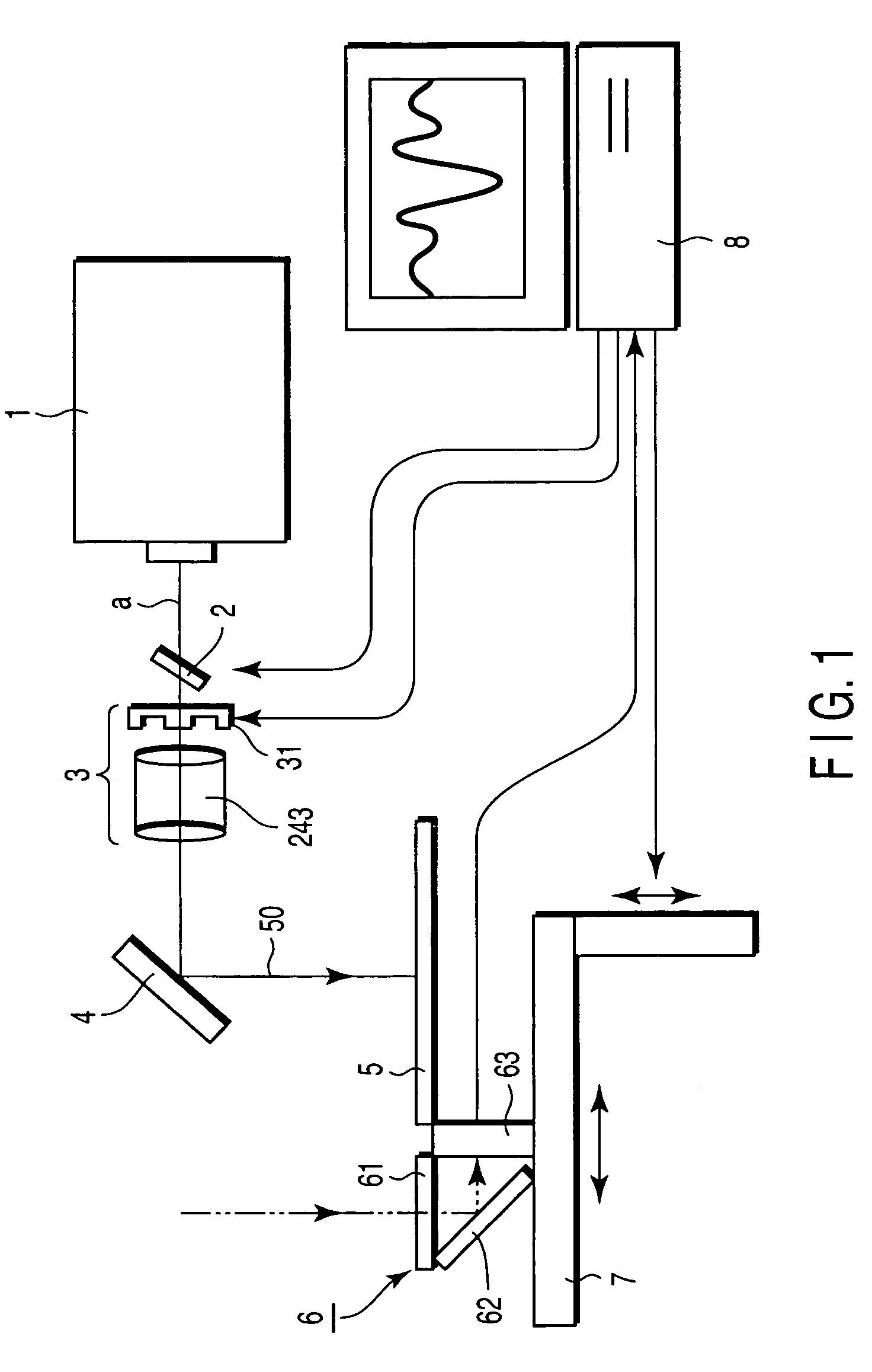
[0108]FIG. 1 is a schematic view showing a laser crystallization apparatus embodying the present invention. In a laser crystallization apparatus, an attenuator 2 and a beam profile modulation portion 3 are arranged at a starting end of an optical axis a of a laser beam source 1 containing the homogenization optical system, and a semiconductor substrate 5 is provided at a trailing end through a mirror 4. Further, a beam profile measurement portion 6 is provided to be aligned with the semiconductor substrate 5, and the semiconductor substrate 5 and the beam profile measurement portion 6 are fixed to a moving stage 7.

[0109]Furthermore, a control personal computer 8 as a controller is set, the beam profile measurement portion 6 is connected on an input side of the personal computer 8, and control systems of the attenuator 2, the beam profile modulation porti...


PUM

PropertyMeasurementUnit
thicknessaaaaaaaaaa
thicknessaaaaaaaaaa
thicknessaaaaaaaaaa

Abstract

There are provided a crystallization method which can design laser beam having a light intensity and a distribution optimized on an incident surface of a substrate, form a desired crystallized structure while suppressing generation of any other undesirable structure area and satisfy a demand for low-temperature processing, a crystallization apparatus, a thin film transistor and a display apparatus. When crystallizing a non-single-crystal semiconductor thin film by irradiating laser beam thereto, irradiation light beam to the non-single-crystal semiconductor thin film have a light intensity with a light intensity distribution which cyclically repeats a monotonous increase and a monotonous decrease and a light intensity which melts the non-single-crystal semiconductor. Further, at least a silicon oxide film is provided on a laser beam incident surface of the non-single-crystal semiconductor film.

Description

CROSS-REFERENCE TO RELATED APPLICATIONS[0001]This application is based upon and claims the benefit of priority from prior Japanese Patent Applications No. 2003-189093, filed Jun. 30, 2003; No. 2003-193779, filed Jul. 8, 2003; No. 2003-308935, filed Sep. 1, 2003; No. 2003-402197, filed Dec. 1, 2003; and No. 2004-093200, filed Mar. 26, 2004, the entire contents of all of which are incorporated herein by reference.BACKGROUND OF THE INVENTION[0002]1. Field of the Invention[0003]The present application relates to a technique to manufacture a field effect transistor at a surface layer part of a non-single-crystal semiconductor thin film, and to single-crystal or polycrystal semiconductor thin film substrate used to manufacture a field effect transistor, and to crystallization method, a crystallization apparatus, a thin film transistor and a display apparatus suitable for manufacture of a display apparatus such as a liquid crystal or an organic EL or an electronic apparatus such as an info...

Claims


Application Information

Patent Timeline
Patent Type & Authority Patents(United States)
IPC IPC(8): H01L21/84G02F1/136B23K26/06C30B13/24H01L21/20H01L21/336H01L21/77H01L29/786
CPCB23K26/063B23K26/0639B23K26/0648C30B13/24H01L21/2026B23K26/0656H01L29/78675H01L27/1285H01L29/66757Y10T117/1008Y10T117/1004B23K26/064B23K26/0622B23K26/066H01L21/02686H01L21/02488H01L21/02422H01L21/02678H01L21/02532H01L21/0242H01L21/02595H01L21/02691G02F1/136
Inventor JYUMONJI, MASAYUKIOGAWA, HIROYUKIMATSUMURA, MASAKIYOHIRAMATSU, MASATOKIMURA, YOSHINOBUTANIGUCHI, YUKIOKATO, TOMOYA
Owner SHARP KK
Why Eureka
Try Eureka