Method of forming metal layer used in the fabrication of semiconductor device

a metal layer and semiconductor technology, applied in the direction of coatings, metallic material coating processes, chemical vapor deposition coatings, etc., can solve the problems of poor step coverage, forth new problems, worse coverage, etc., and achieve the effects of increasing the supplying time of hydrogen gas, increasing the plasma reaction energy, and increasing the plasma reaction energy

Active Publication Date: 2008-08-26
SAMSUNG ELECTRONICS CO LTD
View PDF11 Cites 42 Cited by
  • Summary
  • Abstract
  • Description
  • Claims
  • Application Information

AI Technical Summary

Problems solved by technology

But size reduction of these parts brings forth new problems.
Sputtering, however, has a drawback in that it results in poor step coverage by the metal layer within a contact hole having a high depth-to-opening aspect ratio.
That is, the deeper the hole and the narrower the opening, the worse the coverage by sputtering upto a predetermined height from the bottom of the contact hole.
Furthermore, an insufficient metal silicide layer is formed on the bottom of the contact hole without a subsequent annealing process.
At this time, if a high RF power is used in forming the metal layer, the gate electrode connected to the metal layer or the interlayer insulating layer is charged by the RF power, so that a gate insulating layer formed below the gate electrode may be damaged.
However, the conventional method of forming a metal layer without RF power has problems as follows.
Application of high temperature, however, may damage the semiconductor device and reduce the production yield for such devices during mass manufacturing.
Secondly, premature bonding of the hydrogen and silicon to the surface of the polysilicon or silicon substrate may occur in the PECVD process to portions exposed by the contact hole 311.
The bonded hydrogen and silicon acts as defects in forming metal silicide which results in an increase in the contact resistances of the conductive layer and the metal layer so that electrical characteristics of a semiconductor device may be deteriorated.

Method used


Image

  • Method of forming metal layer used in the fabrication of semiconductor device
  • Method of forming metal layer used in the fabrication of semiconductor device
  • Method of forming metal layer used in the fabrication of semiconductor device

Examples


first embodiment

[0048]FIG. 4 is a flow chart schematically illustrating a method of forming the titanium layer 210 according to the present invention.

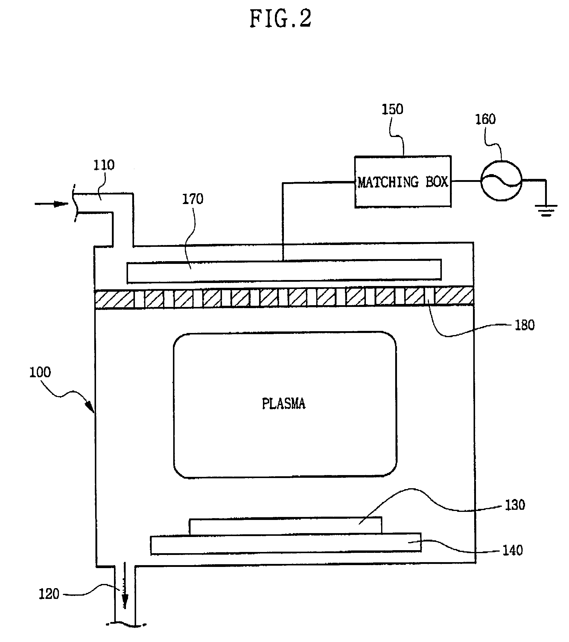
[0049]As shown in FIG. 4, a mixture gas including hydrogen and metal chloride compound (TiCl4) and a purge gas are supplied concurrently for a predetermined time into the sealed chamber 100 (FIG. 2), thereby forming a first titanium layer on the exposed conductive layer of a semiconductor substrate 130 using a PECVD method (S100).

[0050]Here, the first titanium layer is composed of titanium silicide at the interface of the conductive region 200 or the contact pad, and is formed with a predetermined thickness at a temperature necessary to form metal silicide.

[0051]For example, the first titanium layer may be formed with a thickness of about 30 Å by flowing an argon gas at about 300 sccm, a hydrogen gas at about 2000 sccm, and a metal chloride compound gas at about 3 to 5 sccm inside the chamber 100 for about 5 to 6 seconds. At this time, a pressure of t...

second embodiment

[0061]FIG. 7 is a flow chart schematically illustrating a method of forming a titanium layer according to the present invention.

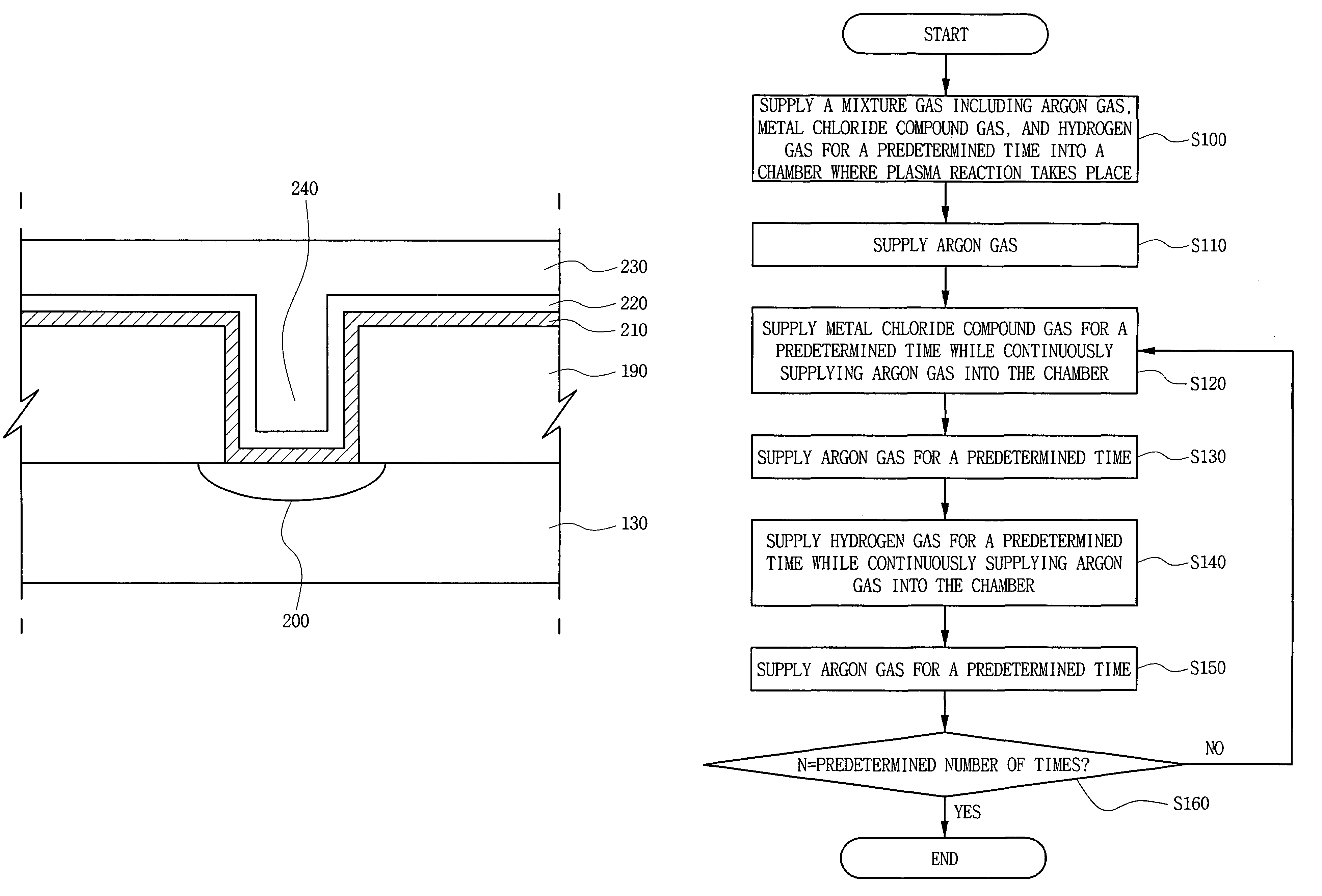
[0062]Referring to FIG. 7, the method of forming a titanium layer 210 according to a second embodiment of the present invention includes flowing only an argon gas at a predetermined flow rate for a predetermined time (S200).

[0063]Then, while the argon gas is continuously flowed into the chamber 100, a metal chloride compound gas is supplied for a predetermined time (S210). Then, the supplying of the metal chloride compound gas is stopped, and only the argon gas is flowed into the chamber 100 for a predetermined time (S220). Then, while the argon gas is continuously flowed, the hydrogen gas is supplied for a predetermined time (S230), thereby forming the titanium layer 210.

[0064]Then, the supplying of the hydrogen gas is stopped, and only the argon gas is flowed into the chamber 100 for a predetermined time. The metal chloride compound gas and the hydrogen g...

third embodiment

[0070]FIG. 9 is a flow chart schematically illustrating a method of forming a titanium layer according to the present invention.

[0071]Referring to FIG. 9, in the method of forming the titanium layer 210 according to a third embodiment of the present invention, only the argon gas is flowed at a predetermined flow rate inside the chamber 100 for a predetermined time with a predetermined RF power (S300). For example, about 200 W of RF power is applied to the upper electrode 170 to induce plasma reaction inside the chamber 100.

[0072]Then, while the argon gas is continuously flowed into the chamber 100, the metal chloride compound gas is supplied for a predetermined time (S310). Then, the supplying of the metal chloride compound gas is stopped, and only the argon gas is flowed into the chamber 100 for a predetermined time (S320). In the same way, about 200 W of RF power is applied to the upper electrode 170 to induce plasma reaction inside the chamber 100. Then, the argon gas is continuo...


PUM

PropertyMeasurementUnit
purge timeaaaaaaaaaa
temperatureaaaaaaaaaa
frequencyaaaaaaaaaa

Abstract

A method of forming a metal layer on the conductive region of a semiconductor device includes concurrently supplying a mixture gas including a hydrogen gas and a metal chloride compound gas, and a purge gas into a chamber having a sealed space for a predetermined time, thereby forming a first metal layer on the semiconductor substrate, using a plasma enhanced chemical vapor deposition (PECVD) method. The hydrogen gas and metal chloride gases are thereafter alternately supplied for a predetermined time while the purge gas is continuously supplied into the chamber, thereby forming a second metal layer on the first metal layer, using a PECVD method. Deterioration of semiconductor devices due to high heat by a conventional CVD method can be prevented using a PECVD method as a low temperature process, thereby improving a production yield.

Description

CROSS-REFERENCE TO RELATED APPLICATION[0001]This application claims the benefit of Korean Patent Application No. 10-2004-0082027, filed Oct. 14, 2004, the disclosure of which is hereby incorporated herein by reference in its entirety.BACKGROUND OF THE INVENTION[0002]1. Technical Field[0003]The present invention relates to a method of fabricating a semiconductor device, and more particularly, to a method of forming a metal layer in the fabrication of a semiconductor device.[0004]2. Discussion of Related Art[0005]With improvements in semiconductor manufacturing, design rules for such devices are continually being scaled down. Accordingly, the elements forming such devices—including transistor channel length, interconnection width and distance, and contact pad size—are getting smaller and smaller.[0006]But size reduction of these parts brings forth new problems. Contact pads, for instance, need to provide a low resistance contact but resistance increases and the part size is reduced. T...

Claims


Application Information

Patent Timeline
Patent Type & Authority Patents(United States)
IPC IPC(8): H01L21/44
CPCC23C16/14C23C16/4408C23C16/45523H01L21/76846H01L21/28556H01L21/76843C23C16/509
Inventor LEE, HYUN-SUKKIM, HYUN-YOUNGMOON, KWANG-JIN
Owner SAMSUNG ELECTRONICS CO LTD
Why Eureka
Try Eureka