Method for preparing alligatored surface of light-emitting diode by using PS spheres as template

A technology for light-emitting diodes and roughened surfaces, which can be used in semiconductor devices, electrical components, circuits, etc., and can solve problems such as poor tolerance of photoresist, difficulty in developing, photolithographic patterns and large wavelengths, etc.

Inactive Publication Date: 2010-02-24
SHANDONG UNIV
View PDF3 Cites 30 Cited by
  • Summary
  • Abstract
  • Description
  • Claims
  • Application Information

AI Technical Summary

Problems solved by technology

However, dry etching requires the fabrication of mask structures
At present, photolithography technology is used most in the semiconductor manufacturing process. However, photolithog

Method used


Image

  • Method for preparing alligatored surface of light-emitting diode by using PS spheres as template
  • Method for preparing alligatored surface of light-emitting diode by using PS spheres as template
  • Method for preparing alligatored surface of light-emitting diode by using PS spheres as template

Examples


Embodiment 1

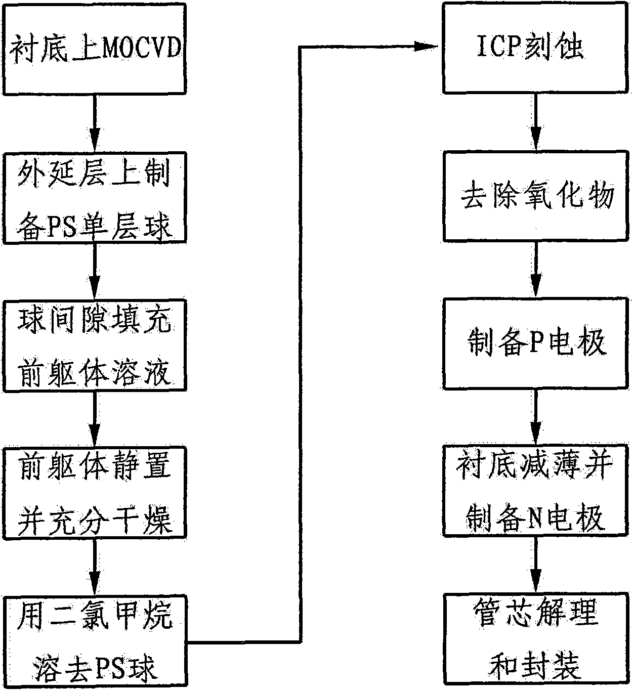
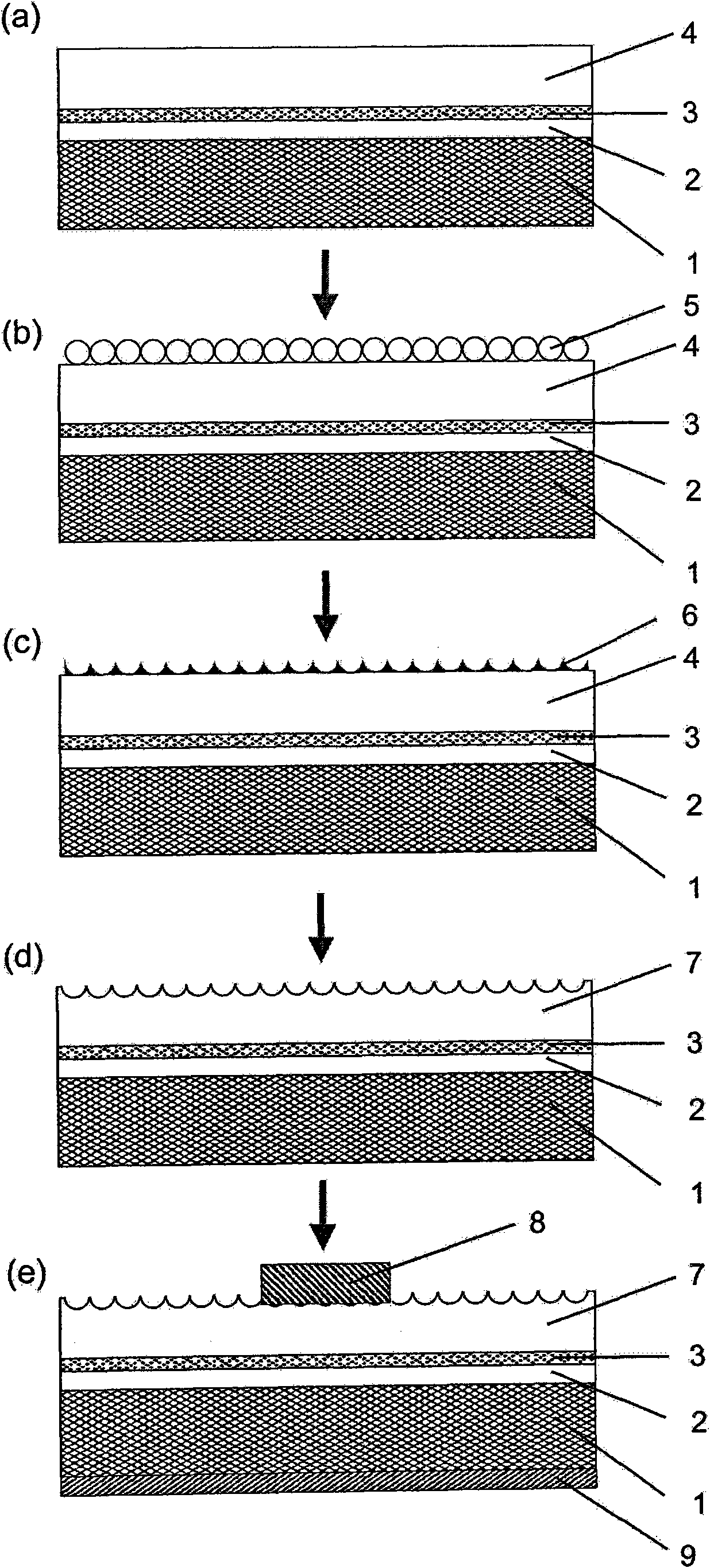
[0022] Such as figure 1 and figure 2 As shown in the flow chart of the operation steps of the present invention and the illustrations, the method of the present invention using PS balls as a template to make a rough surface of a light-emitting diode specifically includes the following steps:

[0023] (1) First, the N-type contact layer 2, the multi-quantum well active region 3 and the P-type contact layer 4 are epitaxially grown on the substrate 1 by metal-organic chemical vapor deposition according to the conventional LED epitaxial growth method to form an epitaxial wafer. Among them, the substrates of red and yellow LEDs are GaAs materials, and the substrates of blue LEDs are Si, GaN or SiC materials. The substrate 1 in this embodiment is a GaAs substrate. see figure 2 Figure (a) in.

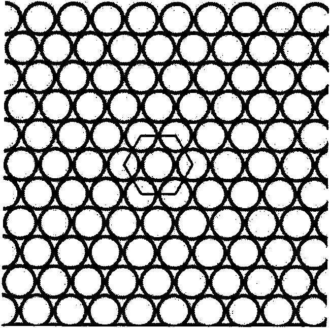
[0024] (2) On the P-type contact layer 4 of epitaxial growth, lay a layer of monolayer film that is formed by the close arrangement of PS balls, the diameter of PS balls is 1000nm in the...

Embodiment 2

[0031] The difference between this example and Example 1 is that in step (4), tin chloride is used as a precursor, tin chloride, ethanol and water are mixed in a mass ratio of 1:4:20 and then filled in the PS ball sheet In the gap between the ball of the layer film 5 and the P-type contact layer 4, let the ethanol and water evaporate at room temperature for 72 hours, and place the epitaxial wafer after standing in a drying oven at 500°C for 1 hour to make the chlorine The tin oxide decomposes into tin oxide. Then obtain the periodic bowl-shaped structure of tin oxide in the same way as in Example 1 step (4), etch the P-type contact covered by the bowl-shaped periodic structure of tin oxide in the same way as in Example 1 step (5). Layer 4, finally adopt HF, NH 3 The corrosive liquid mixed with F and water corrodes the residual tin oxide to obtain a periodic structure of the roughened P-type contact layer.

Embodiment 3

[0033]This embodiment is the same as that of Example 1. In step (3), aluminum nitrate is used as the precursor, and aluminum nitrate, ethanol and water are mixed according to the mass ratio of 1:4:20, and then filled in the PS ball sheet. In the gap between the ball of the layer film 5 and the P-type contact layer 4, let the ethanol and water evaporate at room temperature for 72 hours, place the epitaxial wafer after standing in a drying oven at 500°C for 1 hour, and let the nitric acid Aluminum breaks down to alumina. Then obtain the periodically arranged bowl-shaped structure of aluminum oxide by the same method of embodiment 1 step (4), etch the P-type contact covered by the bowl-shaped periodic arrangement structure of tin oxide by the same method of embodiment 1 step (5) Layer 4, finally adopt HF, NH 3 The corrosive solution mixed with F and water corrodes the residual aluminum oxide to obtain a periodic structure of the coarsened P-type contact layer.

[0034] Chloride...


PUM

PropertyMeasurementUnit
Diameteraaaaaaaaaa

Abstract

The invention provides a method for preparing an alligatored surface of a light-emitting diode by using PS spheres as template. The method comprises the following steps: (1) performing epitaxial growth according to the conventional method to prepare an epitaxial wafer; (2) paving a layer of one-layer film which comprises closely packed PS spheres on the P-type contact layer obtained through epitaxial growth; (3) mixing precursor which is tetraethyl silicate, metal chloride or metal nitrate with ethanol and water to fill in the gap of the PS spheres of the one-layer film and the P-type contactlayer, standing at room temperature, heating to decompose the mixture and obtain the related oxides; (4) placing the epitaxial wafer in dichloromethane to dissolve the PS spheres, preserving the formed oxides in the gap of the PS spheres and the P-type contact layer on the P-type contact layer according to bowl-shaped periodic arrangement structure; (5) using the formed oxides as mask to perform dry etching on the P-type contact layer and obtain the alligatored surface; and (6) corroding and removing the residual oxides. The invention can be used to prepare the alligatored surface of the light-emitting diode with controllable etching period and depth.

Description

technical field [0001] The invention relates to a method for making a rough surface of a light-emitting diode by using a polystyrene (PS) ball as a template, and belongs to the technical field of light-emitting diode production. Background technique [0002] Semiconductor light-emitting diodes (LEDs) have been widely used in LED indicator lights, LED traffic lights, and LED display screens since their invention. With the development of semiconductor technology, the efficiency of LEDs is constantly improving, but more improvements are necessary in terms of electro-optical conversion efficiency. [0003] In principle, there are two ways to increase the efficiency of LEDs. The first way is to improve the internal quantum efficiency, which depends on the epitaxial crystal quality and epitaxial structure; the second way is to improve the light extraction efficiency. For GaP-based red LEDs, the internal quantum efficiency is already very high, even close to 100%. There is little...

Claims


Application Information

Patent Timeline
IPC IPC(8): H01L33/00
Inventor 郝霄鹏夏伟巩海波吴拥中徐现刚
Owner SHANDONG UNIV
Why Eureka
Try Eureka