Objective lens, electron beam system and method of inspecting defect

a technology of electron beam and lens, applied in the direction of instruments, magnetic discharge control, nuclear engineering, etc., can solve the problems of axial magnetic distribution, inability to obtain high resolution images, and large number of ampere turns (ats) needed for operating lenses, etc., to achieve good edge roughness and high yield rate

Inactive Publication Date: 2008-09-02
EBARA CORP
View PDF6 Cites 49 Cited by
  • Summary
  • Abstract
  • Description
  • Claims
  • Application Information

AI Technical Summary

Benefits of technology

[0016]An electrostatic lens has been used for an objective lens in a conventional optical system in order to improve a throughput, which is arranged so as to project secondary electrons emitted from a sample onto a detector by forming multiple beams and scanning the sample therewith. Therefore, such a conventional system has suffered from the problem of aberration becoming large and as a result a large beam current cannot be obtained when the beams are narrowed down to a smaller size. The present invention has the object, accordingly, to provide an objective lens that comprises a magnetic lens having a lens gap on the sample side, which can narrow down the multiple beams to a smaller size and obtain a large beam current.
[0189]In the repair method as described firstly in the present invention 4-3, a secondary electronic signal can be used at the time of obtaining the SEM image, the secondary electronic signal being obtained by absorbing electrons in an electrode which are generated as a result of secondary electron multiplication that is caused to occur upon collision of the secondary electrons with gases. In the repair method as described firstly in the present invention 4-3, it is advantageous to use a signal used for the detection of the secondary electrons, when the SEM image is to be obtained, which are accelerated and condensed in an electric field formed on the mask and the pressure control aperture, passed through them, and deflected toward the secondary electron detector with an ExB separator. In the repair method as described firstly in the present invention 4-3, the pressure and kind of the gas on the mask can be changed at the time of repairing and obtaining the SEM image. Further, the present invention 4-3 can provide a device production method for the production of a device characterized in that lithography is carried out by using the mask which is repaired by either of the methods as described above.

Problems solved by technology

The objective lens, however, has the problem that a number of ampere turns (ATs) needed for operating lenses becomes larger.
Further, the objective lens presents the problem that a distribution of an axial magnetic distribution cannot be obtained at a necessary level for the reasons that a magnetic flux density within a magnetic pole becomes too large due to a remote distance between the position of the magnetic gap and the position of the beam passing therethrough, thereby saturating a magnetic permeability of a magnetic material and as a result gaining no necessary distribution of the axial magnetic field.
Therefore, the magnetic lens has the problem that no NA aperture can be disposed at the cross-over position so that no image having a high resolution can be obtained.
In other words, the problem resides in that, in the event where the NA aperture is disposed at the cross-over position, electrons coming from a position apart from the optical axis is blocked to an extent more than needed, thereby darkening an image at the neighboring portion.
Therefore, such a conventional system has suffered from the problem of aberration becoming large and as a result a large beam current cannot be obtained when the beams are narrowed down to a smaller size.
Moreover, if a magnetic field exists on a sample, beams coming out vertically from the sample do not cross the optical axis so that no NA aperture can be disposed and that, as a result, a crosstalk between a secondary beam and the adjacent beam becomes large.

Method used


Image

  • Objective lens, electron beam system and method of inspecting defect
  • Objective lens, electron beam system and method of inspecting defect
  • Objective lens, electron beam system and method of inspecting defect

Examples


first embodiment

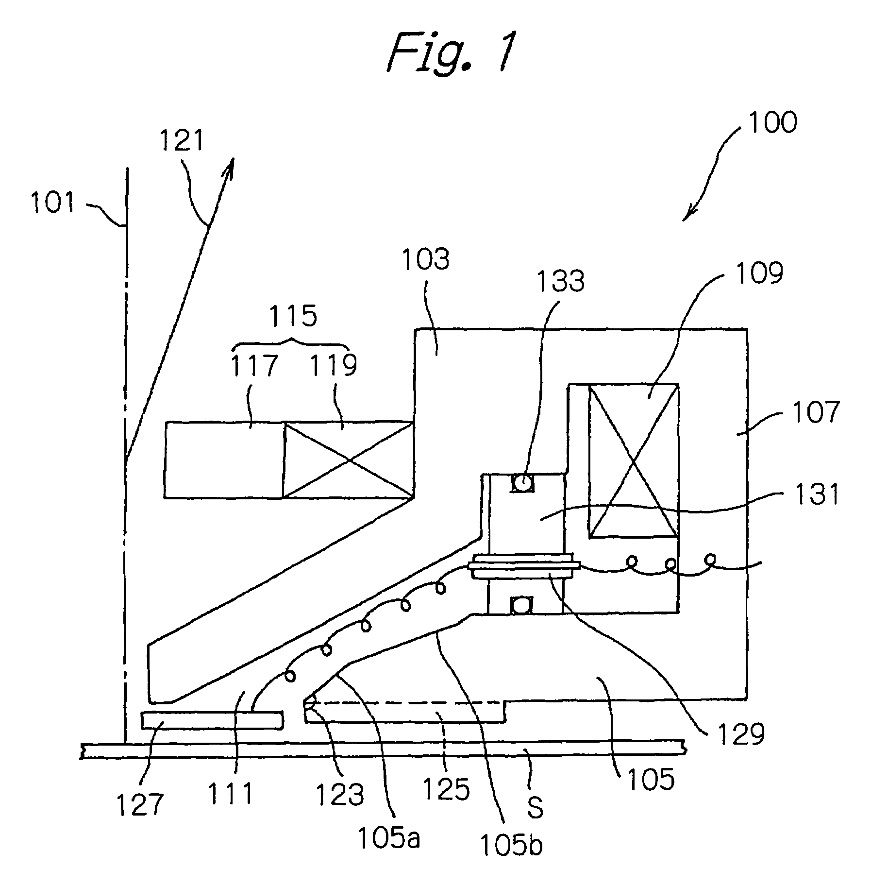
[0230]FIG. 1 shows a cross-sectional shape of an objective lens system 100 to be used for an electron beam system in accordance with the present invention 1-1. An actual structure of the objective lens system 100 can be represented by rotating it around the optical axis 101. An electron gun is disposed at an upper side of FIG. 1, although not shown herein, and primary electron beams generated from the electron gun are focused onto the surface of a sample S through the optical axis with the objective lens system 100. The objective lens system has a structure surrounding the exciting coil 109 with the inner magnetic pole 103 disposed on the side of the optical axis, the outer magnetic pole 105 disposed on the side opposite thereto, and the magnetic circuit 107, and it is arranged such that the lens gap 111 is located having an aperture directed toward sample S. Reference numeral 115 refers to a beam separator for deflecting secondary electrons to be emitted from the sample toward samp...

second embodiment

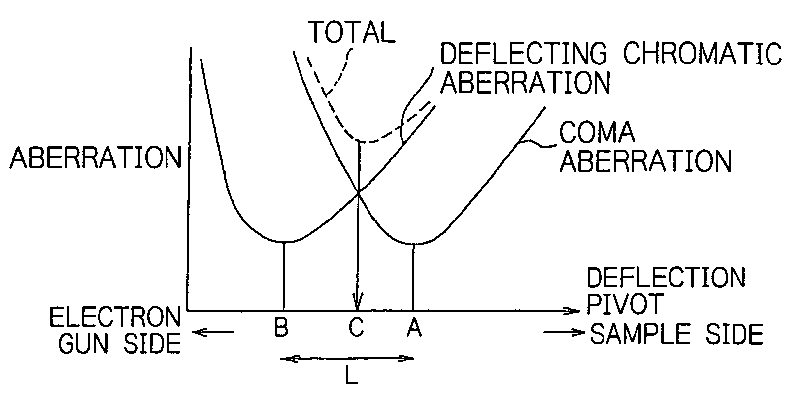
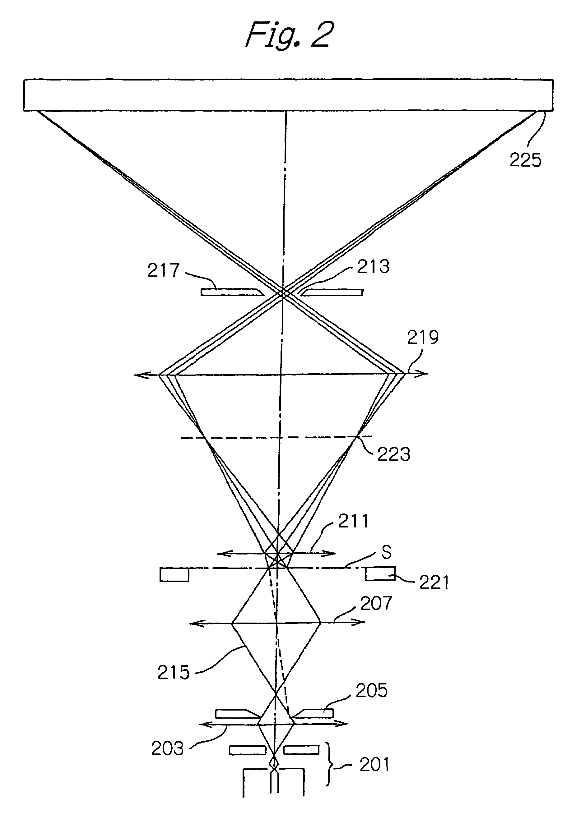
[0237]FIG. 2 shows an optical system of an inspection apparatus for a transmission mask using the objective lens system according to the present invention. The optical system of the inspection apparatus may be disposed in such a manner that the LaB6 cathode electron gun 201 is operated under space-charge limit conditions, electrons generated from the electron gun 201 are condensed with the condenser lens 203, the shaping rectangular aperture 205 are irradiated with the electron beams at a homogeneous intensity, and an image is formed on a stencil mask (sample) 209 with the irradiating lens 207. Then, a cross-over image formed with the electron gun is formed on a principal plane of the objective lens 211. The objective lens 211 is set to have a still larger axial magnetic field at the position of the sample S. Therefore, the electrons emitted in the normal direction from the sample S do not cross the optical axis at a cross-over 213.

[0238]Hitherto, the principal light beams from the ...

third embodiment

[0243]FIG. 3 shows an embodiment in which the objective lens according to the present invention 1-3 is used for an optical system for irradiation with multi-beams. The electron gun 301 is arranged such that a LaB6 cathode electron gun is operated under space-charge limit conditions in substantially the same manner as described in the embodiment as shown in FIG. 2. The electron beams emitted from the electron gun 301 form a cross-over at the NA aperture 307 in an association of the condenser lens 303 with the rotating lens 305 whose rotation can be adjusted. Multiple beams are formed by mounting the multi-aperture 309 in front of the rotating lens 305. The condenser lens 303 adjusts a density of beam current at the multi-aperture by varying a cross-over magnification at the NA aperture 307 without forming a cross-over in association with the lens 305 disposed adjacent thereto. In the optical system, all the lenses are needed to align the posture of the multiple beams with the ordinat...


PUM


Abstract

An electron beam system or a method for manufacturing a device using the electron beam system in which an electron beam can be irradiated at a high current density and a ratio of transmittance of a secondary electron beam of an image projecting optical system can be improved and which can be compact in size. The surface of the sample S is divided into plural stripe regions which in turn are divided into rectangle-shaped main fields. The main field is further divided into plural square-shaped subfields. The irradiation with the electron beams and the formation of a two-dimensional image are repeated in a unit of the subfields. A magnetic gap formed by the inner and outer magnetic poles of the objective lens is formed on the side of the sample, and an outer side surface and an inner side surface of each of the inner magnetic pole and the outer magnetic pole, respectively, forming the magnetic gap have each part of a conical shape with a convex having an angle of 45° or greater with respect to the optical axis.

Description

TECHNICAL FIELD[0001]The present invention relates to a high throughput apparatus for evaluating a sample having a pattern with a minimum line width of 0.1 μm or less including, for example, a pattern on a substrate, a method for the evaluation of a pattern thereon and an objective lens for using the same.[0002]The present invention also relates to an electron beam system and a method for the manufacturing of a device by using the same and, more particularly, to a apparatus for evaluating a sample including, but not being limited to a patterned wafer, a mask for forming a pattern, a substrate for use with a liquid crystal panel or a micromachine product, etc. with both a high precision and a high throughput and to a method for manufacturing a device by using the electron beam system.[0003]The present invention further relates to a method for evaluating including inspecting etc. a defect on a sample having a pattern with a minimum line width of 0.2 μm or less with a high throughput a...

Claims


Application Information

Patent Timeline
Patent Type & Authority Patents(United States)
IPC IPC(8): H01J1/50H01J37/141H01J37/28
CPCH01J37/141H01J2237/28H01J2237/1534
Inventor NAKASUJI, MAMORUSATAKE, TOHRUSOBUKAWA, HIROSIMURAKAMI, TAKESHIWATANABE, KENJINOJI, NOBUHARU
Owner EBARA CORP
Why Eureka
Try Eureka