Nonvolatile semiconductor memory device having a gate stack and method of manufacturing the same

a semiconductor memory and gate stack technology, applied in the field of semiconductor memory devices, can solve the problems of low retention characteristic of flash memory, data cannot be kept safe, and the speed of writing/erasing data becomes much slower than the desired speed, so as to achieve effective control of trap density and increase the operating speed

Active Publication Date: 2008-09-02
SAMSUNG ELECTRONICS CO LTD
View PDF36 Cites 17 Cited by
  • Summary
  • Abstract
  • Description
  • Claims
  • Application Information

AI Technical Summary

Benefits of technology

[0023]A nonvolatile memory device according to the present invention provides the capability of controlling trap density effectively according to the doping concentration. Accordingly, writing / erasing of data can be operated at a lower voltage than in the conventional art, thereby increasing the operating speed as compared to the conventional art.

Problems solved by technology

However, the flash memory has a low retention characteristic and data stored therein cannot be kept safely for a long period of time due to a leakage current.
If a low operating voltage is applied to the conventional SONOS device, the speed of writing / erasing of data becomes much slower than a desired speed.
Due to such voltage dependence characteristic, the control of a trap density of the nitride film 14 also becomes difficult.
The retention time also is not sufficiently long.
These drawbacks arise due to the high thickness of the films required by the use of nitride and silicon oxide, which have low dielectric constants.
However, the applied voltage is still very high and it is still difficult to control the trap density of the silicon nitride film.

Method used


Image

  • Nonvolatile semiconductor memory device having a gate stack and method of manufacturing the same
  • Nonvolatile semiconductor memory device having a gate stack and method of manufacturing the same
  • Nonvolatile semiconductor memory device having a gate stack and method of manufacturing the same

Examples


first embodiment

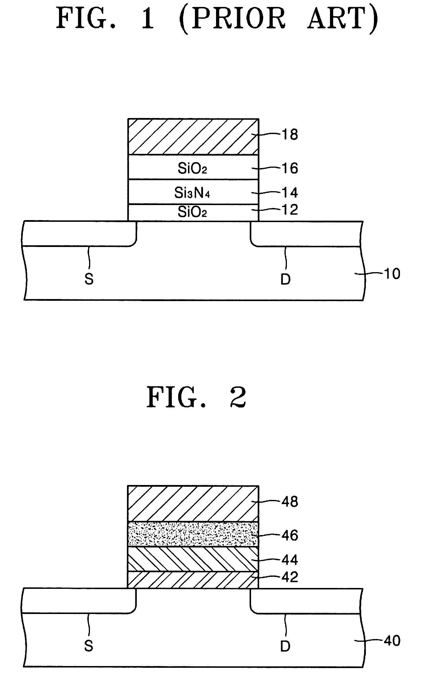
[0037]Referring to FIG. 2, a source region S and drain region D are formed on a substrate 40 and separated by a predetermined distance. A space between the source region S and the drain region D on the substrate 10 defines a channel region. A gate stack is formed on the channel region. The gate stack is formed of the following layers deposited sequentially. First, a tunneling oxide film 42 is provided on the channel region. One end of the tunneling oxide film 42 contacts the source region S and another end of the tunneling oxide film 42 contacts the drain region D. A first trapping material layer 44 is formed on the tunneling oxide film 42. A first insulating film 46 having a high dielectric constant is formed on the first trapping material layer 44. Finally, a gate electrode 48 is formed on the first insulating film 46.

[0038]When a predetermined voltage is applied to the gate electrode 48 and the drain region D, the first trapping material film 44 traps a charge, i.e., electrons, w...

second embodiment

[0042]The second embodiment is related to a nonvolatile semiconductor memory device having a diffusion barrier layer on and under the first trapping material film 44.

[0043]In the following, the same reference numerals as in the first embodiment describe the same elements.

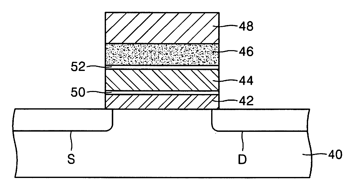
[0044]Referring to FIG. 3, a first oxide film 50, serving as a first diffusion barrier layer, is formed between the tunneling oxide film 42 and the first trapping material film 44. The first oxide film 50 may be an aluminum oxide film. The thickness of the tunneling oxide film 42 may be approximately 1˜4 nm, and that of the first oxide film 50 may be approximately 0.5˜2 nm. The phrase “tunneling film” as used herein is defined as the tunneling oxide film 42 in combination with the first oxide film 50.

[0045]A second oxide film 52, serving as a second diffusion barrier layer, is formed between the first trapping material film 44 and the first insulating film 46. The second oxide film 52 may be an aluminum oxide film, ...

third embodiment

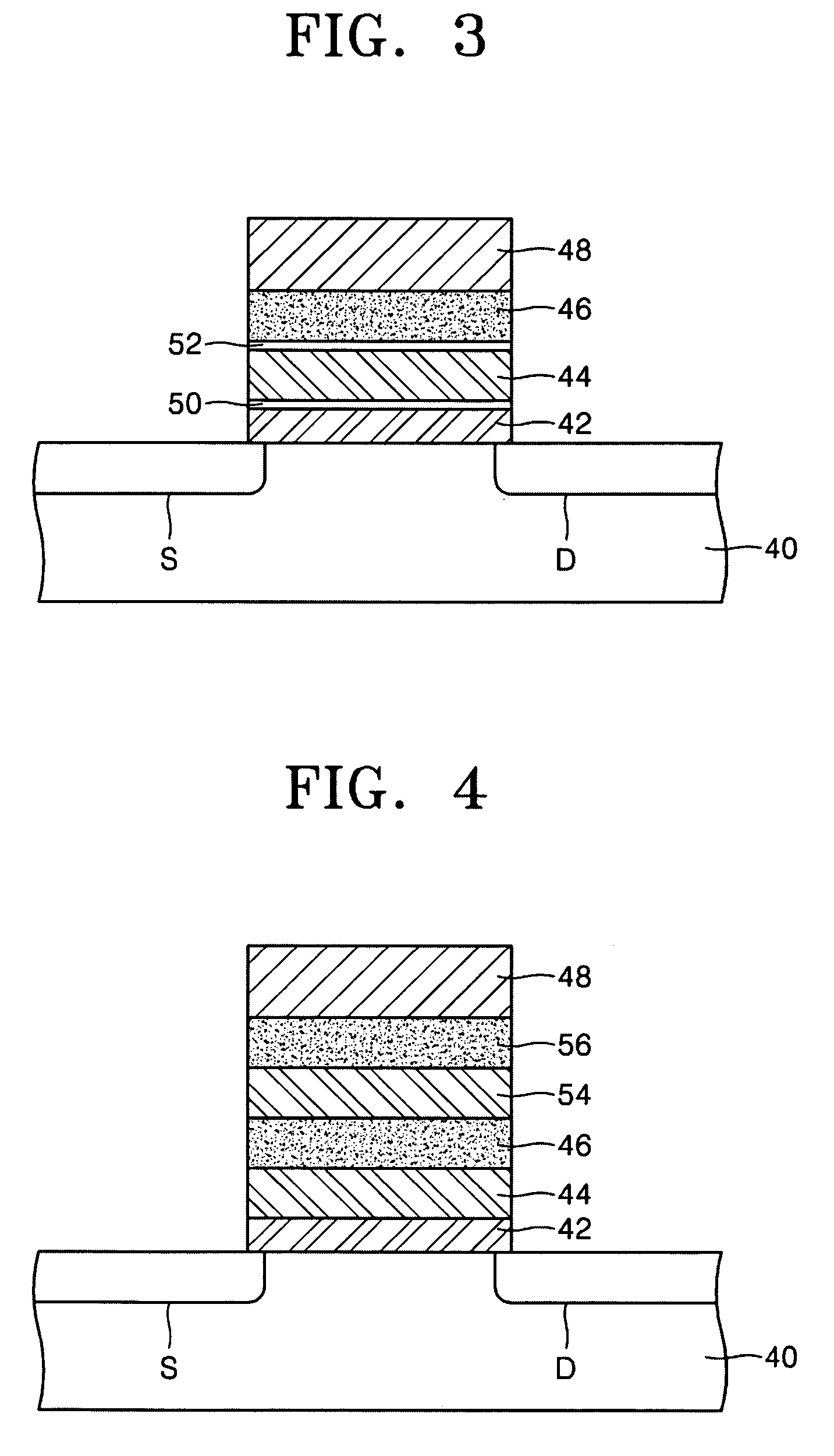
[0047]The third embodiment is related to a nonvolatile semiconductor memory device including a gate stack formed on a channel region of a substrate 40 and having a plurality of trapping material films.

[0048]Referring to FIG. 4, the first trapping material film 44 and the first insulating film 46 are formed on the tunneling oxide film 42. A second trapping material film 54 and a second insulating film 56 are sequentially deposited on the first insulating film 46. The gate electrode 48 is formed on the second insulating film 56. The second trapping material film 54 may be formed of an insulating film of doped lanthanide having a high dielectric constant, e.g., of the same material as that of the first trapping material film 44. Alternatively, the second trapping material film 54 may be formed of other insulating films. Likewise, the second insulating film 56 may be formed of the same insulating material film as the first insulating film 46. Alternatively, the second insulating film 56...


PUM


Abstract

A nonvolatile semiconductor memory device includes a semiconductor substrate having a source region and a drain region, and a gate stack formed on the semiconductor substrate between and in contact with the source and drain regions. The gate stack includes, in sequential order from the substrate: a tunneling film; a first trapping material film doped with a first predetermined impurity, the first trapping material film having a higher dielectric constant than the nitride film (Si3N4); a first insulating film having a higher dielectric constant than a nitride film; and a gate electrode. Such a nonvolatile semiconductor memory device can effectively control the trap density according to the doping concentration, thereby increasing the write/erase speed of data at a low operating voltage.

Description

BACKGROUND OF THE INVENTION[0001]1. Field of the Invention[0002]The present invention relates to a semiconductor memory device. More particularly, the present invention relates to a nonvolatile semiconductor memory device having a gate with a different film structure from a silicon-oxide / nitride / oxide-silicon (SONOS), and a method of manufacturing the same.[0003]2. Description of Related Art[0004]Recent developments of portable data storage devices, such as memory sticks, that readily allow data sharing and exchange regardless of hardware type have led to increased demands regarding safe storage of large amounts of data. One possible solution is a flash memory device, i.e., a special type of an electrically erasable programmable read-only memory (EEPROM), which can be erased or programmed in blocks of data and the contents of which are retained even when the power is turned off. The flash memory device generally has a multi-layer structure including a floating gate, where a charge i...

Claims


Application Information

Patent Timeline
Patent Type & Authority Patents(United States)
IPC IPC(8): H01L29/76H01L29/788H01L29/792H01L29/94H01L31/062H01L31/113H01L31/119H01L21/8247H01L21/28H01L21/336H01L21/8246H01L27/115H01L27/11568H01L29/51
CPCH01L21/28194H01L21/28282H01L29/792H01L29/517H01L29/518H01L29/66833H01L29/513H01L27/11568H01L29/40117H10B43/30H10B99/00
Inventor CHAE, SOO-DOOKIM, CHUNG-WOOLEE, JUNG-HYUNKIM, MOON-KYUNGHWANG, HYUN-SANG
Owner SAMSUNG ELECTRONICS CO LTD
Why Eureka
Try Eureka